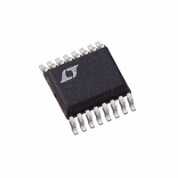
LTC1646CGN Linear Technology, LTC1646CGN Datasheet - Page 11

LTC1646CGN
Manufacturer Part Number
LTC1646CGN
Description
IC CNTRLR HOTSWAP PCIDUAL 16SSOP
Manufacturer
Linear Technology
Type
Hot-Swap Controllerr
Datasheet
1.LTC1646CGNPBF.pdf
(20 pages)
Specifications of LTC1646CGN
Applications
CompactPCI™
Internal Switch(s)
No
Voltage - Supply
3.3V, 5V
Operating Temperature
0°C ~ 70°C
Mounting Type
Surface Mount
Package / Case
16-SSOP (0.150", 3.90mm Width)
Lead Free Status / RoHS Status
Contains lead / RoHS non-compliant
Available stocks
Company
Part Number
Manufacturer
Quantity
Price
Company:
Part Number:
LTC1646CGN
Manufacturer:
LT
Quantity:
10 000
Part Number:
LTC1646CGN
Manufacturer:
LT/凌特
Quantity:
20 000
Part Number:
LTC1646CGN#PBF
Manufacturer:
LT/凌特
Quantity:
20 000
Part Number:
LTC1646CGN#TR
Manufacturer:
LT/凌特
Quantity:
20 000
Part Number:
LTC1646CGN#TRPBF
Manufacturer:
LINEAR/凌特
Quantity:
20 000
APPLICATIO S I FOR ATIO
Power-Down Sequence
When BD_SEL# is pulled high, a power-down sequence
begins (Figure 3).
Internal switches are connected to each of the output
supply voltage pins to discharge the bypass capacitors to
ground. The TIMER pin (Pin 2) is immediately pulled low.
The GATE pin (Pin 10) is pulled down by a 200µA current
source to prevent the load currents on the 3.3V and 5V
supplies from going to zero instantaneously in order to
prevent glitching the power supply voltages. When either
of the output voltages dips below its threshold, HEALTHY#
pulls high and LOCAL_PCI_RST# will be asserted low.
Once the power-down sequence is complete, the CPCI
card may be removed from the slot. During extraction, the
precharge circuit will continue to bias the bus I/O pins at
1V until the 5V and 3.3V long connector pin connections
are separated.
Timer
During a power-up sequence, a 5µA current source is
connected to the TIMER pin and current limit faults are
ignored until the voltage exceeds 1.25V. This feature
LCL_PCI_RST#
PRECHARGE
HEALTHY#
BD_SEL#
10V/DIV
5V/DIV
5V/DIV
5V/DIV
5V/DIV
5V/DIV
5V/DIV
TIMER
5V
3V
GATE
OUT
OUT
Figure 2. Normal Power-Up Sequence
U
U
20ms/DIV
W
U
1646 F02
allows the chip to power up CPCI boards with widely
varying capacitive loads on the supplies. The power-up
time for either of the two outputs is given by:
Where XV
C
5V
variables in Equation 2 with the appropriate values, the
turn-on time for the 3V
The timer period should be set longer than the maximum
supply turn-on time but short enough to not exceed the
maximum safe operating area of the pass transistor during
a short-circuit. The timer period for the LTC1646 is given
by:
As a design aid, the timer period as a function of the timing
capacitor using standard values from 0.01µF to 1µF is
shown in Table 2.
LOAD
LCL_PCI_RST#
OUT
t
t
ON
TIMER
PRECHARGE
HEALTHY#
BD_SEL#
(5V
10V/DIV
(
turn-on time will be ~10ms. By substituting the
5V/DIV
5V/DIV
5V/DIV
5V/DIV
5V/DIV
5V/DIV
TIMER
5V
3V
XV
GATE
OUT
OUT
OUT
=
OUT
Figure 3. Normal Power-Down Sequence
OUT
C
) = 2000µF, I
TIMER
)
= 2
= 5V
5
µ
•
• . 1 25
A
I
OUT
LIMIT XVOUT
OUT
C
LOAD XVOUT
LIMIT
or 3V
V
(
output can also be calculated.
(
10ms/DIV
= 7A, and I
OUT
)
–
. For example, for
I
)
LOAD XVOUT
•
LTC1646
XV
(
LOAD
OUT
= 5A, the
)
11
1646 F03
1646fa
(2)
(3)


