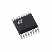
LTC1646CGN Linear Technology, LTC1646CGN Datasheet - Page 17

LTC1646CGN
Manufacturer Part Number
LTC1646CGN
Description
IC CNTRLR HOTSWAP PCIDUAL 16SSOP
Manufacturer
Linear Technology
Type
Hot-Swap Controllerr
Datasheet
1.LTC1646CGNPBF.pdf
(20 pages)
Specifications of LTC1646CGN
Applications
CompactPCI™
Internal Switch(s)
No
Voltage - Supply
3.3V, 5V
Operating Temperature
0°C ~ 70°C
Mounting Type
Surface Mount
Package / Case
16-SSOP (0.150", 3.90mm Width)
Lead Free Status / RoHS Status
Contains lead / RoHS non-compliant
Available stocks
Company
Part Number
Manufacturer
Quantity
Price
Company:
Part Number:
LTC1646CGN
Manufacturer:
LT
Quantity:
10 000
Part Number:
LTC1646CGN
Manufacturer:
LT/凌特
Quantity:
20 000
Part Number:
LTC1646CGN#PBF
Manufacturer:
LT/凌特
Quantity:
20 000
Part Number:
LTC1646CGN#TR
Manufacturer:
LT/凌特
Quantity:
20 000
Part Number:
LTC1646CGN#TRPBF
Manufacturer:
LINEAR/凌特
Quantity:
20 000
APPLICATIO S I FOR ATIO
Since there is no bulk capacitance to damp the parasitic
trace inductance, supply voltage transients excite para-
sitic resonant circuits formed by the power MOSFET
capacitance and the combined parasitic inductance from
the wiring harness, the backplane and the circuit board
traces. These ringing transients appear as a fast edge on
the 3.3V or 5V supply, exhibiting a peak overshoot to 2.5
times the steady-state value followed by a damped sinu-
soidal response whose duration and period is dependent
on the resonant circuit parameters. Since the absolute
maximum supply voltage of the LTC1646 is 10V, transient
protection against 3.3V and 5V supply voltage spikes and
ringing is highly recommended.
In these applications, there are two methods for eliminat-
ing these supply voltage transients: using Zener diodes to
clip the transient to a safe level and snubber networks.
Snubbers are RC networks whose time constants are
large enough to safely damp the inductance of the board’s
parasitic resonant circuits. As a starting point, the shunt
capacitors in these networks are chosen to be 10× to 100×
the power MOSFET’s C
series resistor (R6 and R7 in Figure 13) is then chosen to
be large enough to damp the resulting series R-L-C circuit
and typically ranges from 1Ω to 10Ω. Note that in all
LONG 3.3V
LONG 5V
U
3.3V
V
V
IN1
IN2
5V
OSS
Z1, Z2: BZX84C6V2
**ADDITIONAL DETAILS OMITTED FOR CLARITY
U
0.1µF
Z1
C2
under bias. The value of the
R6 2.7Ω
R7 1.8Ω
Figure 13. Place Transient Protection Device Close to the LTC1646
W
3V
IN
8
0.005Ω
R1
3V
SENSE
U
9
IRF7413
GATE
Q2
10
R3
10Ω
3V
LTC1646**
OUT
7
GND
LTC1646 circuit schematics, Zener diodes and snubber
networks have been added to each 3.3V and 5V supply rail
and should be used always. These protection networks
should be mounted very close to the LTC1646’s supply
voltage using short lead lengths to minimize lead induc-
tance. This is shown schematically in Figure 13 and a
recommended layout of the transient protection devices
around the LTC1646 is shown in Figure 14.
6
5V
*ADDITIONAL DETAILS OMITTED FOR CLARITY
DRAWING IS NOT TO SCALE!
IN
0.007Ω
12
R2
5V
LTC1646*
SENSE
Figure 14. Recommended Layout for
Transient Protection Components
11
IRF7413
Q1
R4
10Ω
5V
5V
IN
OUT
GND
5
R5
1k
3V
IN
0.01µF
C1
C3
0.1µF
Z2
1646 F13
TZ2
5V
AT 5A
3V
AT 7.6A
TZ1
OUT
OUT
LTC1646
1646 F14
C2
C3
VIAS TO
GND PLANE
17
1646fa


