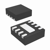
LTC4361IDC-1#TRPBF Linear Technology, LTC4361IDC-1#TRPBF Datasheet - Page 12

LTC4361IDC-1#TRPBF
Manufacturer Part Number
LTC4361IDC-1#TRPBF
Description
IC CTLR OVP LATCHOFF 8DFN
Manufacturer
Linear Technology
Type
Overvoltage and Overcurrent Controllerr
Datasheet
1.LTC4361CDC-2TRMPBF.pdf
(16 pages)
Specifications of LTC4361IDC-1#TRPBF
Applications
General Purpose
Internal Switch(s)
No
Voltage - Supply
2.5 V ~ 5.5 V
Operating Temperature
-40°C ~ 85°C
Mounting Type
Surface Mount
Package / Case
8-WFDFN Exposed Pad
Lead Free Status / RoHS Status
Lead free / RoHS Compliant
Available stocks
Company
Part Number
Manufacturer
Quantity
Price
LTC4361-1/LTC4361-2
APPLICATIONS INFORMATION
Figure 8 shows a particularly severe situation which can
occur in a mobile device with dual power inputs. A 20V wall
adaptor is mistakenly hot-plugged into the 5V device with
the USB input already live. As shown in Figure 9, a large
current can build up in L
N-channel MOSFET shuts off, the energy stored in L
dumped into C
LTC4361 limits this to a 1V rise in the output voltage.
If the ∆V
C
MOSFET is exceeded, an additional external clamp such
as the SMAJ24A can be placed between IN and GND. C
is the decoupling capacitor of the protected circuits and
its value will largely be determined by their requirements.
Using a larger C
dV/dt at OUT, allowing time for the LTC4361 to shut off the
12
ADAPTER
OUT
WALL
USB
20V
Figure 8. Setup for Testing 20V Plugged into 5V System
5V
is not acceptable or the avalanche capability of the
OUT
+
+
–
–
R
IN
due to the discharge of the energy in L
I
OUT
CABLE
OUT
L
IN
, causing a large 40V input transient. The
will work with L
IN
B160
D1
to charge up C
IN R
R1
100k
SENSE
Figure 10. Layout for N-Channel MOSFET Confi guration
IN
SENSE
IN
to slow down the
Si1470DH
LTC4361
GATE
GND
M1
OUT
OUT
SUPPLY
. When the
LTC4361
IN
R
OUT
SENSE
IN
436112 F08
C
into
OUT
OUT
is
LOAD
IN
Si1470DH
MOSFET before V
A larger C
discharge of the energy in L
used as an input clamp.
Layout Considerations
Figure 10 shows an example PCB layout for the LTC4361
(TS8 package) with a single N-channel MOSFET (SC70
package) and a 0603 size sense resistor. Keep the traces
to the N-channel MOSFET wide and short. The PCB traces
associated with the power path through the N-channel
MOSFET should have low resistance. Use Kelvin connec-
tions to R
436112 F10
20V/DIV
10V/DIV
10A/DIV
5V/DIV
I
V
CABLE
GND
OUT
V
Figure 9. Overvoltage Protection Waveforms
When 20V Plugged into 5V System
SENSE
GATE
OUT
OUT
V
IN
FIGURE 8 CIRCUIT
R
L
C
also helps to lower the ∆V
IN
OUT
IN
for an accurate overcurrent threshold.
= 2μH, R
= 150mΩ
= 10μF (16V, SIZE 1210)
OUT
overshoots to a dangerous voltage.
SENSE
= 25mΩ, LOAD = 10Ω
1μs/DIV
IN
if the MOSFET BV
436112 F09
OUT
due to the
DSS
436112fa
is


