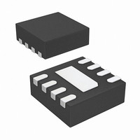
LTC4361IDC-1#TRPBF Linear Technology, LTC4361IDC-1#TRPBF Datasheet - Page 9

LTC4361IDC-1#TRPBF
Manufacturer Part Number
LTC4361IDC-1#TRPBF
Description
IC CTLR OVP LATCHOFF 8DFN
Manufacturer
Linear Technology
Type
Overvoltage and Overcurrent Controllerr
Datasheet
1.LTC4361CDC-2TRMPBF.pdf
(16 pages)
Specifications of LTC4361IDC-1#TRPBF
Applications
General Purpose
Internal Switch(s)
No
Voltage - Supply
2.5 V ~ 5.5 V
Operating Temperature
-40°C ~ 85°C
Mounting Type
Surface Mount
Package / Case
8-WFDFN Exposed Pad
Lead Free Status / RoHS Status
Lead free / RoHS Compliant
Available stocks
Company
Part Number
Manufacturer
Quantity
Price
APPLICATIONS INFORMATION
ON Input
ON is a CMOS compatible, active low enable input. It has
a default 5μA pull-down to ground. Connect this pin to
ground or leave open to enable normal device operation.
If it is driven high while the external MOSFET is turned on,
GATE is pulled low with a weak pull-down current (40μA)
to turn off the external MOSFET gradually, minimizing input
voltage transients. The LTC4361 then goes into a low cur-
rent sleep mode, drawing only 1.5μA at IN. When ON goes
back low, the part restarts with a 130ms delay cycle.
GATEP Control
GATEP has a 2M resistive pull-down to ground and a 5.8V
Zener clamp in series with a 200k resistor to IN. It con-
trols the gate of an optional external P-channel MOSFET
to provide negative voltage protection. The 2M resistive
pull-down turns on the MOSFET once V
more than the MOSFET gate threshold voltage. The IN to
GATEP Zener protects the MOSFET from gate overvoltage
by clamping its V
MOSFET Confi gurations and Selection
The LTC4361 can be used with various external MOSFET
confi gurations (see Figure 3). The simplest confi guration
is a single N-channel MOSFET. It has the lowest R
and voltage drop and is thus the most power effi cient
solution. When GATE is pulled to ground, the N-channel
MOSFET can isolate OUT from a positive voltage at IN up
to the BV
current can still fl ow from OUT to IN via the parasitic body
diode of the N-channel MOSFET.
DSS
of the N-channel MOSFET. However, reverse
GS
to 5.8V when V
IN
goes high.
IN
– V
GATEP
DS(ON)
is
For near zero reverse-leakage current protection when GATE
is pulled to ground, back-to-back N-channel MOSFETs
can be used. Adding an additional P-channel MOSFET
controlled by GATEP provides negative input voltage
protection down to the BV
Another confi guration consists of a P-channel MOSFET
controlled by GATEP and a N-channel MOSFET controlled
by GATE. This provides protection against overvoltage and
negative voltage but not reverse current.
SUPPLY
SUPPLY
SUPPLY
SUPPLY
PROTECTION
PROTECTION
NEGATIVE
NEGATIVE
VOLTAGE
VOLTAGE
GATEP
GATEP
M2
M2
LTC4361-1/LTC4361-2
Figure 3. MOSFET Confi gurations
IN
IN
IN
IN
R
R
R
R
SENSE
SENSE
SENSE
SENSE
DSS
SENSE
SENSE
SENSE
SENSE
of the P-channel MOSFET.
OVERVOLTAGE
OVERVOLTAGE, REVERSE-
OVERVOLTAGE, REVERSE-
PROTECTION
OVERVOLTAGE
CURRENT PROTECTION
CURRENT PROTECTION
PROTECTION
GATE
GATE
GATE
GATE
M1
M1
M1
M1
M3
M3
436112 F03
436112fa
OUT
OUT
OUT
OUT
9


