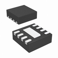
LTC4361IDC-1#TRPBF Linear Technology, LTC4361IDC-1#TRPBF Datasheet - Page 5

LTC4361IDC-1#TRPBF
Manufacturer Part Number
LTC4361IDC-1#TRPBF
Description
IC CTLR OVP LATCHOFF 8DFN
Manufacturer
Linear Technology
Type
Overvoltage and Overcurrent Controllerr
Datasheet
1.LTC4361CDC-2TRMPBF.pdf
(16 pages)
Specifications of LTC4361IDC-1#TRPBF
Applications
General Purpose
Internal Switch(s)
No
Voltage - Supply
2.5 V ~ 5.5 V
Operating Temperature
-40°C ~ 85°C
Mounting Type
Surface Mount
Package / Case
8-WFDFN Exposed Pad
Lead Free Status / RoHS Status
Lead free / RoHS Compliant
Available stocks
Company
Part Number
Manufacturer
Quantity
Price
PIN FUNCTIONS
Exposed Pad (DFN): Ground. Connection to PCB is optional.
GATE: Gate Drive for External N-Channel MOSFET. An
internal charge pump provides a 10μA pull-up current
to charge the gate of the external N-channel MOSFET. An
additional ramp circuit limits the GATE ramp rate when
turning on to 3V/ms. For slower ramp rates, connect an
external capacitor from GATE to GND. An internal clamp
limits GATE to 6V above the OUT pin voltage. An internal
GATE high comparator controls the PWRGD pin.
GATEP: Gate Drive for External P-Channel MOSFET. GATEP
connects to the gate of an optional external P-channel
MOSFET to protect against negative voltages at IN. This pin
is internally clamped to 5.8V below V
tor connects this pin to ground. Connect to IN if not used.
GND: Device Ground.
IN: Supply Voltage Input. Connect this pin to the input
power supply. This pin has an overvoltage threshold of
5.8V. After an overvoltage event, this pin must fall below
BLOCK DIAGRAM
ON
5μA
1V
IN
+
–
. An internal 2M resis-
CONTROL
CHARGE
PUMP
OVERCURRENT
COMPARATOR
OVERVOLTAGE
COMPARATOR
10μA
GND
+
–
V
ing lockout, GATE is held low and the PWRGD pull-down
releases.
ON: On Control Input. A logic low at ON enables the LTC4361.
A logic high at ON activates a low current pull-down at the
GATE pin and causes the LTC4361 to enter a low current
sleep mode. An internal 5μA current pulls ON down to
ground. Connect to ground or leave open if unused.
OUT: Output Voltage Sense Input for GATE Clamp. Connect
to the source of the external N-channel MOSFET to sense
the output voltage for GATE to OUT clamp.
PWRGD: Power Good Status. Open-drain output with
internal 500k resistive pull-up to OUT. Pulls low 65ms
after GATE ramps above V
SENSE: Current Sense Input. Connect a sense resistor
between IN and SENSE. An overcurrent protection circuit
turns off the N-channel MOSFET when the voltage across
the sense resistor exceeds 50mV for more than 10μs.
200k
1.8M
GATEP
+
IN(OV)
COMPARATOR
50mV
GATE HIGH
+
–
+
–
–
5.8V
– ∆V
V
GATE(TH)
LTC4361-1/LTC4361-2
OV
5.8V
5.7V
to release the overvoltage lockout. Dur-
IN
SENSE
GATE(TH)
500k
PWRGD
5.8V
GATE
OUT
436112 BD
.
436112fa
5


