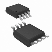
LM5068MMX-3/NOPB National Semiconductor, LM5068MMX-3/NOPB Datasheet - Page 12

LM5068MMX-3/NOPB
Manufacturer Part Number
LM5068MMX-3/NOPB
Description
IC CTLR HOT SWAP -48V 8-MSOP
Manufacturer
National Semiconductor
Type
Hot-Swap Controllerr
Datasheet
1.LM5068MM-3NOPB.pdf
(26 pages)
Specifications of LM5068MMX-3/NOPB
Applications
General Purpose
Internal Switch(s)
No
Voltage - Supply
-10 V ~ -90 V
Operating Temperature
-40°C ~ 105°C
Mounting Type
Surface Mount
Package / Case
8-TSSOP, 8-MSOP (0.118", 3.00mm Width)
Linear Misc Type
Negative Voltage
Family Name
LM5068-3
Package Type
MSOP
Operating Supply Voltage (min)
-10V
Operating Supply Voltage (max)
-90V
Operating Temperature (min)
-40C
Operating Temperature (max)
105C
Operating Temperature Classification
Industrial
Product Depth (mm)
3mm
Product Height (mm)
0.86mm
Product Length (mm)
3mm
Mounting
Surface Mount
Pin Count
8
For Use With
LM5068EVAL - EVALUATION BOARD FOR LM5068
Lead Free Status / RoHS Status
Lead free / RoHS Compliant
Other names
LM5068MMX-3
Available stocks
Company
Part Number
Manufacturer
Quantity
Price
Company:
Part Number:
LM5068MMX-3/NOPB
Manufacturer:
TI
Quantity:
25
www.national.com
Current Control
conditions. The voltage drop across the sense resistor (R
is monitored at the SENSE pin. The over-current protection
functions are determined through the following three distinct
thresholds at the SENSE pin:
1. Circuit Breaker (CB) threshold (typically 50mV)
2. Analog Current Limit (ACL) loop threshold (typically
3. Fast Discharge Current (FDC) threshold (typically
When the voltage drop across R
Breaker comparator indicates an over-load condition. The
TIMER sources 240µA into C
and sinks 6µA from C
C
declared and the gate of the MOSFET is forced low, discon-
necting the power to the load.
Active Current Limiting (ACL) is activated when the voltage
across sense resistor R
trols the gate of the MOSFET and maintains a constant
output load current equal to 100mV/ R
SENSE pin is greater than 50mV and the TIMER charges C
with 240µA. A fault will be declared if the LM5068 remains in
the ACL mode longer than the circuit breaker timer period.
Fast Discharge Current (FDC) responds to fast rising over-
loads such as short circuit faults. During a short circuit event
the fast rising current may overshoot past the ACL threshold
due to the finite response time of the ACL loop. If the SENSE
voltage reaches 200mV a fast discharge comparator quickly
pulls GATE pin low. The rapid response of the FDC circuit
assures a fast and safe transition to the ACL mode.
The LM5068 circuit breaker action filters low duty cycle
over-load conditions to avoid declaring a fault during short
duration load transients. The timer charges capacitor C
240µA when the SENSE voltage is greater than 50mV. When
the SENSE pin voltage falls below 50mV, a 6µA current
discharges the TIMER capacitor. Repetitive over-current
faults with duty cycle greater than 2.5% will eventually
charge C
pass MOSFET which has a fast heating and slow cooling
characteristic.
Latch-Off and Auto-Retry
If the fault conditions persist long enough for TIMER to
charge C
switches off and initiates the re-try timer (LM5068-2, -4).
At the fault condition, after reaching the 4V, the TIMER pin
will continue to ramp-up with 6µA current source until it
reaches the internal regulated voltage, which is equivalent to
the saturation GATE drive voltage. The LM5068-1 and
LM5068-3 remains off until the controller is reset by either
temporarily pulling the UV pin low, pulling the TIMER pin
below 1 volt, or decreasing the input voltage below the
internal V
The LM5068-2 and LM5068-4 respond to a fault condition by
pulling the GATE and TIMER pins low and then initiating a
timer sequence for automatic re-try. The re-try timer se-
quence begins with C
with a 6µA current source and then discharged quickly to 1V
with a 30mA discharge current. After 8 charge/discharge
cycles the GATE pin is released and charged with a 60µA
T
capacitor ramps to a 4V threshold, a fault condition is
100mV)
200mV)
T
T
DD
and trip the fault timer. This feature protects the
to 4V, the LM5068 latches off (LM5068-1, -3) or
under-voltage lockout (UVLO) threshold.
T
T
when SENSE falls below 50mV. If the
capacitor being charged slowly to 4V
S
reaches 100mV. The LM5068 con-
(Continued)
T
when SENSE exceeds 50mV
S
exceeds 50mV the Circuit
S
. In the ACL mode the
T
with
S
T
)
12
current source. If the fault condition persists, the LM5068 will
again turn off the MOSFET and another 8-cycle fault timer
sequence will begin.
Power Good Flag
The power good flag (PWRGD) is activated when the MOS-
FET GATE is fully enhanced (
and OV comparators are satisfied. The power good output is
a 90V capable open drain N-Channel MOSFET. The
LM5068-1 and LM5068-2 provide an active HIGH power-
good state, while the LM5068-3 and LM5068–4 are config-
ured for an active LOW power-good state. The UV compara-
tor, OV comparator, V
will reset the power good flag.
Internal Soft-Start
An internal soft-start feature ramps the (positive) input of the
analog current limit amplifier during initial start-up. The ramp
duration is approximately 200µs. This feature reduces the
load current slew rate (di/dt) at start-up.
Design Information
The LM5068 contains an internal regulator enabling the V
pin to be connected directly to the line voltage from 10 to
90V. A local RC filter (0.1µF ceramic capacitor and 499Ω
resistor) connected between V
to filter supply transients that exceed the 100V Absolute
Maximum Rating.
UV and OV Thresholds and
Voltage Divider Selection for R1,
R2, and R3
Two comparators detect under-voltage and over-voltage
conditions at the UV and OV pins. The threshold voltages
(V
2.5V. Hysteresis is accomplished by 20µA current sources
(I
UV and OV pins as shown in Figure 3
UVHCS
UV
, V
), into the external resistor divider connected to the
OV
) of the UV and OV comparators are nominally
FIGURE 3. UV/OV Setting
DD
UVLO, or a circuit breaker time-out
>
DD
8V) and the voltage input UV
and V
EE
is recommended
20078606
DD


