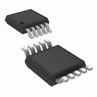
LM5067MMX-2/NOPB National Semiconductor, LM5067MMX-2/NOPB Datasheet - Page 15

LM5067MMX-2/NOPB
Manufacturer Part Number
LM5067MMX-2/NOPB
Description
IC CTLR NEG HOTSWAP A/R 10MSOP
Manufacturer
National Semiconductor
Type
Hot-Swap Controllerr
Datasheet
1.LM5067MM-1NOPB.pdf
(24 pages)
Specifications of LM5067MMX-2/NOPB
Applications
General Purpose
Internal Switch(s)
No
Voltage - Supply
-9 V ~ -80 V
Operating Temperature
-40°C ~ 125°C
Mounting Type
Surface Mount
Package / Case
10-TFSOP, 10-MSOP (0.118", 3.00mm Width)
Linear Misc Type
Negative Voltage
Family Name
LM5067-2
Package Type
MSOP
Operating Supply Voltage (min)
-9V
Operating Supply Voltage (max)
-80V
Operating Temperature (min)
-40C
Operating Temperature (max)
125C
Operating Temperature Classification
Automotive
Product Depth (mm)
3mm
Product Height (mm)
0.86mm
Product Length (mm)
3mm
Mounting
Surface Mount
Pin Count
10
For Use With
LM5067EVAL - NEGATIVE HOT SWAP / INRUSH CURRE
Lead Free Status / RoHS Status
Lead free / RoHS Compliant
Other names
LM5067MMX-2
Available stocks
Company
Part Number
Manufacturer
Quantity
Price
Company:
Part Number:
LM5067MMX-2/NOPB
Manufacturer:
TI
Quantity:
4 500
(R
value is calculated from:
where I
voltage across R
modulates the gate of Q1 to regulate the current at I
the current limiting circuit is active, the fault timer is active as
described in the Fault Timer & Restart section. For proper
operation, R
While the maximum load current in normal operation can be
used to determine the required power rating for resistor R
basing it on the current limit value provides a more reliable
design since the circuit can operate near the current limit
threshold continuously. The resistor’s surge capability must
also be considered since the circuit breaker threshold is ap-
proximately twice the current limit threshold. Connections
from R
niques. In the suggested layout of Figure 7 the small pads at
the upper corners of the sense resistor connect only to the
sense resistor terminals, and not to the traces carrying the
high current. With this technique, only the voltage across the
sense resistor is applied to VEE and SENSE, eliminating the
voltage drop across the high current solder connections.
POWER LIMIT THRESHOLD
The LM5067 determines the power dissipation in the external
MOSFET (Q1) by monitoring the drain current (the current in
R
the PWR pin (R
Q1, and is calculated from the following equation:
where P
and R
Limit section. For example, if R
power limit threshold is 60W, R
Q1’s power dissipation reaches the power limit threshold,
Q1’s gate is modulated to control the load current, keeping
Q1’s power from exceeding the threshold. For proper opera-
tion of the power limiting feature, R
While the power limiting circuit is active, the fault timer is ac-
S
S
), and the V
), connected from SENSE to VEE. The required resistor
S
S
LIM
is the current sense resistor described in the Current
FET(LIM)
to the LM5067 should be made using Kelvin tech-
FIGURE 7. Sense Resistor Connections
R
is the desired current limit threshold. When the
PWR
S
must be no larger than 100 mΩ.
DS
PWR
= 1.42 x 10
is the desired power limit threshold for Q1,
of Q1 (OUT to SENSE pins). The resistor at
S
) sets the maximum power dissipation for
reaches 50 mV, the current limit circuit
5
x R
S
PWR
S
is 10 mΩ, and the desired
x P
calculates to 85.2 kΩ. If
PWR
FET(LIM)
must be
≤
LIM
150 kΩ.
30030935
. While
(1)
(2)
S
,
15
tive as described in the Fault Timer & Restart section. Typi-
cally, power limit is reached during startup, or when the V
of Q1 increases due to a severe overload or short circuit.
The programmed maximum power dissipation should have a
reasonable margin relative to the maximum power defined by
the SOA chart if the LM5067-2 is used since the FET will be
repeatedly stressed during fault restart cycles. The FET man-
ufacturer should be consulted for guidelines. The PWR pin
can be left open if the application does not require use of the
power limit function.
TURN-ON TIME
The output turn-on time depends on whether the LM5067 op-
erates in current limit only, or in both power limit and current
limit, during turn-on.
A) Turn-on with current limit only: If the current limit thresh-
old is less than the current defined by the power limit threshold
at maximum V
threshold during turn-on. Referring to Figure 10a, as the drain
current reaches I
at V
reaches its final value (V
to the value defined by the load, and the gate is charged to
approximately 13V (V
to transition from zero volts to V
where C
C
maximum instantaneous power dissipated in the MOSFET is
48W. This calculation assumes the time from t1 to t2 in Figure
10a is small compared to t
current until after the output voltage has reached its final val-
ue, and PGD switches high (Figure 8).
If the load draws current during the turn-on sequence (Figure
9), the turn-on time is longer than the above calculation, and
is approximately equal to:
where R
of the system input voltage. The Fault Timeout Period must
be set longer than t
the turn-on sequence is complete.
L
= 1000 µF, and I
GSL
FIGURE 8. No Load Current During Turn-on
to maintain the current at I
L
L
is the load capacitance. For example, if V
is the load resistance and V
DS
LIM
the circuit operates only at the current limit
, the gate-to-source voltage is controlled
ON
LIM
GATE
to prevent a fault shutdown before
= 1A, t
DS
ON
). The time for the OUT pin voltage
≊
, and the load does not draw any
0V) the drain current reduces
ON
SYS
LIM
calculates to 48 ms. The
is equal to:
SYS
. As the output voltage
is the absolute value
30030937
www.national.com
SYS
= -48V,
DS


