LM5067MWX-1/NOPB National Semiconductor, LM5067MWX-1/NOPB Datasheet - Page 12
LM5067MWX-1/NOPB
Manufacturer Part Number
LM5067MWX-1/NOPB
Description
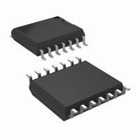
IC CTLR NEG HOTSWAP LATCH 14SOIC
Manufacturer
National Semiconductor
Type
Hot-Swap Controllerr
Datasheet
1.LM5067MM-1NOPB.pdf
(24 pages)
Specifications of LM5067MWX-1/NOPB
Applications
General Purpose
Internal Switch(s)
No
Voltage - Supply
-9 V ~ -80 V
Operating Temperature
-40°C ~ 125°C
Mounting Type
Surface Mount
Package / Case
14-SOIC (0.300", 7.50mm Width)
Lead Free Status / RoHS Status
Lead free / RoHS Compliant
Other names
LM5067MWX-1
Available stocks
Company
Part Number
Manufacturer
Quantity
Price
Company:

Part Number:
LM5067MWX-1/NOPB
Manufacturer:
TI/NS
Quantity:
340


www.national.com
Operating Voltage
The LM5067 operating voltage is the voltage from VCC to
VEE. The maximum operating voltage is set by an internal
13V zener diode. With the IC connected as shown in Figure
1, the LM5067 controller operates in the voltage range be-
tween VEE and VEE+13V. The remainder of the system
voltage is dropped across the input resistor R
be selected to pass at least 2 mA into the LM5067 at the min-
imum system voltage.
Gate Control
The external N-channel MOSFET is turned on when the
GATE pin sources 52 µA to enhance the gate. During normal
operation (t3 in Figure 3) Q1’s gate is held charged to ap-
proximately 13V above VEE, typically within 20 mV of the
voltage at VCC. If the maximum V
13V, a lower voltage external zener diode must be added be-
tween the GATE and SENSE pins. The external zener diode
must have a forward current rating of at least 110 mA.
GS
FIGURE 3. Power Up Sequence (Current Limit only)
rating of Q1 is less than
IN
, which must
12
When the system voltage is initially applied (before the oper-
ating voltage reaches the POR
held low by a 110 mA pull-down current. The pull-down cur-
rent helps prevent an inadvertent turn-on of the MOSFET
through its drain-gate capacitance as the applied system volt-
age increases.
During the insertion time (t1 in Figure 3) the GATE pin is held
low by a 2.2 mA pull-down current. This maintains Q1 in the
off-state until the end of t1, regardless of the voltage at VCC
and UVLO.
Following the insertion time, during t2 in Figure 3, the gate
voltage of Q1 is modulated to keep the current or Q1’s power
dissipation level from exceeding the programmed levels. Cur-
rent limiting and power limiting are considered fault condi-
tions, during which the voltage on the TIMER pin capacitor
increases. If the current and power limiting cease before the
TIMER pin reaches 4V the TIMER pin capacitor is discharged,
and the circuit enters normal operation. See the Fault Timer
& Restart paragraph for details on the fault timer.
IT
threshold), the GATE pin is
30030930
Related parts for LM5067MWX-1/NOPB
Image
Part Number
Description
Manufacturer
Datasheet
Request
R

Part Number:
Description:
National Semiconductor [8-Bit D/A Converter]
Manufacturer:
National Semiconductor
Datasheet:
Part Number:
Description:
National Semiconductor [Media Coprocessor]
Manufacturer:
National Semiconductor
Datasheet:
Part Number:
Description:
Digitally Controlled Tone and Volume Circuit with Stereo Audio Power Amplifier, Microphone Preamp Stage and National 3D Sound
Manufacturer:
National Semiconductor
Datasheet:
Part Number:
Description:
Digitally Controlled Tone and Volume Circuit with Stereo Audio Power Amplifier, Microphone Preamp Stage and National 3D Sound
Manufacturer:
National Semiconductor
Datasheet:
Part Number:
Description:
AC97 Rev 2 Codec with Sample Rate Conversion and National 3D Sound
Manufacturer:
National Semiconductor
Part Number:
Description:
Manufacturer:
National Semiconductor
Datasheet:
Part Number:
Description:
Manufacturer:
National Semiconductor
Datasheet:
Part Number:
Description:
General Purpose, Low Voltage, Low Power, Rail-to-Rail Output Operational Amplifiers
Manufacturer:
National Semiconductor
Datasheet:
Part Number:
Description:
8-bit 20 MSPS flash A/D converter.
Manufacturer:
National Semiconductor
Datasheet:
Part Number:
Description:
Low Noise Quad Operational Amplifier
Manufacturer:
National Semiconductor
Datasheet:
Part Number:
Description:
Quad Differential Line Receivers
Manufacturer:
National Semiconductor
Datasheet:
Part Number:
Description:
Quad High Speed Trapezoidal? Bus Transceiver
Manufacturer:
National Semiconductor
Datasheet:
Part Number:
Description:
Dual Line Receiver
Manufacturer:
National Semiconductor
Datasheet:
Part Number:
Description:
TTL to 10k ECL Level Translator with Latch
Manufacturer:
National Semiconductor
Datasheet: