LP3950SL/NOPB National Semiconductor, LP3950SL/NOPB Datasheet
LP3950SL/NOPB
Specifications of LP3950SL/NOPB
LP3950SLTR


Related parts for LP3950SL/NOPB


LP3950SL/NOPB Summary of contents
Page 1
... Typical Application © 2005 National Semiconductor Corporation Features n Audio synchronization for color LEDs with two modes: Amplitude and Frequency n Programmable frequency and amplitude response with ...
Page 2
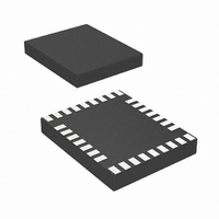
Connection Diagrams and Package Mark Information 32-Lead Thin CSP Package, 4.5 x 5.5 x 0.8 mm, 0.5 mm Pitch Top View Note: The actual physical placement of the package marking will vary from part to part. The package marking “XY” ...
Page 3
Pin Description Pin # Name Type 1 FB Input 2 GND_BOOST Ground 3 SW Output 4 V Power DD2 5 GND2 Ground 6 DME Logic Input 7 AMODE Logic Input 8 V Power DDA 9 ASE Input 10 AD1 Input ...
Page 4
... Note 7: For detailed package and soldering specifications and information, please refer to National Semiconductor Application Note 1125: Laminate CSP/FBGA. Note 8: The Human body model is a 100 pF capacitor discharged through a 1.5 kΩ resistor into each pin. The machine model is a 200 pF capacitor discharged directly into each pin ...
Page 5
Electrical Characteristics Note 9: In applications where high power dissipation and/or poor package thermal resistance is present, the maximum ambient temperature may have to be derated. Maximum ambient temperature (T A-MAX dissipation of the device in the application (P D-MAX ...
Page 6
Block Diagram Modes of Operation RESET: In the RESET mode all the internal registers are reset to the default values. RESET is entered always if input NRST is LOW or internal Power On Reset is active. STANDBY: The STANDBY mode ...
Page 7
Modes of Operation (Continued) Logic Interface Characteristics (1.80V ≤ V ≤ V V). Limits in standard typeface are for T DDIO DD1,2 ambient temperature range (−40˚C ≤ T Symbol Parameter LOGIC INPUTS SS, SI, SCK/SCL, PWM_LED, IF_SEL V Input Low ...
Page 8
Logic Interface Characteristics (1.80V ≤ V ≤ V V). Limits in standard typeface are for T DDIO DD1,2 ambient temperature range (−40˚C ≤ T Symbol Parameter LOGIC INPUTS DME, AMODE (Internal pull down 1 MΩ) I Logic Input Current I ...
Page 9
SPI Interface (Continued) and it has to be taken high between successive cycles. Data is clocked in on the rising edge of the SCK clock signal, while data is clocked out on the falling edge of SCK. FIGURE 2. SPI ...
Page 10
DD1 DD2 DDA Symbol 1 Cycle Time 2 Enable Lead Time 3 Enable Lag Time 4 Clock Low Time 5 Clock High Time 6 Data Setup Time 7 Data Hold Time 8 Data Access Time ...
Page 11
I C Compatible Interface TRANSFERRING DATA Every byte put on the SDA line must be eight bits long, with the most significant bit (MSB) being transferred first. Each byte of data has to be followed by an acknowledge bit. ...
Page 12
I C Compatible Interface ( 2.70V to 2.90V, V DD1 DD2 DDA Symbol 1 Hold Time (repeated) START Condition Clock Low Time (1.65V ≤ Clock Low Time (1.80V ≤ Clock ...
Page 13
Magnetic Boost DC/DC Converter The boost DC/DC converter generates a 4.1V–5.3V output voltage to drive LEDs from a single Li-Ion battery (3.0V to 4.5V). The output voltage is controlled with an eight-bit register in nine steps. The converter is a ...
Page 14
Magnetic Boost DC/DC Converter Electrical Characteristics Limits in standard typeface are for T (−40˚C ≤ T ≤ +85˚C). Unless otherwise noted, specifications apply to Figure 1 with 100 nF, C VDD2 VDDA ...
Page 15
Boost Converter Typical Performance Characteristics otherwise stated. Boost Converter Efficiency Battery Current vs Voltage Boost Typical Waveforms at 100 mA Load Boost Frequency vs RT Resistor 20129316 Battery Current vs Voltage 20129317 Boost Startup with No Load 20129318 15 V ...
Page 16
Boost Converter Typical Performance Characteristics otherwise stated. (Continued) Boost Line Regulation RGB LED Pattern Generator The LP3950 RGB outputs can be controlled either with audio synchronization or with RGB pattern generator. The pattern generator of LP3950 drives three independently controlled ...
Page 17
Programmable Pattern Mode (Continued) FIGURE 14. Example Blinking Waveforms RGB Driver Characteristics (R1, G1, B1, R2, G2, B2 outputs). Limits in standard typeface are for T ating ambient temperature range (−40˚C ≤ T Symbol Parameter R ON Resistance DS-ON I ...
Page 18
RGB LED PWM Control ROFF[3:0] OFF sets the beginning time of the turn-off slope. Off-time is relative to blinking cycle length in the same GOFF[3:0] way as on-time. BOFF[3:0] ROFF[3:0] GOFF[3:0] BOFF[3: OFF = 0 and ...
Page 19
Audio Synchronization The LEDs connected to the RGB outputs can be synchro- nized to incoming audio signal with Audio Synchronization feature. Audio Synchronization has two modes. Amplitude mode synchronizes LEDs based on the peak amplitude of the input signal. In ...
Page 20
Audio Synchronization INPUT BUFFERING Figure 16 describes the LP3950 audio input buffering struc- ture in high level. The electric parameters of the buffers are described in Table Audio Synchronization Characteristics. Operational amplifiers for both buffers are rail-to-rail input opamps. The ...
Page 21
Audio Synchronization Symbol Parameter Zin Input Impedance of AD1, AD2, ASE pins A Audio Input Level Range IN_SINGLE (peak-to-peak), Single Ended Audio A Audio Input Level Range IN_DIFF (peak-to-peak), Differential Audio f Crossover Frequencies (−3 dB Narrow Frequency ...
Page 22
Audio Synchronization FIGURE 18. LP3950 Audio Synchronization Functionality MODE CONTROL IN THE FREQUENCY MODE During the frequency mode (SYNC_MODE = 1) the user can select between two filter options by MODE_CTRL[1:0] as shown below (Figure 19). User can select the ...
Page 23
Audio Synchronization MODE CONTROL IN THE AMPLITUDE MODE During the amplitude synchronization mode (SYNC_MODE = 0) the user can select between three different amplitude mappings by using MODE_CTRL[1:0] select. These three MODE_CTRL[1:0] = [00] = MODE0 MODE_CTRL[1:0] = [01] = ...
Page 24
Audio Synchronization RGB_SEL[0] RGB_SEL[ www.national.com (Continued) RGB Output Control RGB1 Output Control 0 Pattern Generator 0 Audio Sync 1 Pattern Generator 1 Audio Sync 24 RGB2 Output Control Pattern Generator Pattern Generator Audio Sync Audio Sync ...
Page 25
Recommended External Components OUTPUT CAPACITOR, C OUT The output capacitor C directly affects the magnitude of OUT the output ripple voltage. In general, the higher the value the lower the output ripple magnitude. Multilayer ce- OUT ramic ...
Page 26
PCB Design Guidelines capacitor, the inductor, the SW pin, the GND_BOOST pin and the ground plane, as shown by the dashed line in Figure 21. The other switching loop, the rectifier loop, is formed by the input capacitor, the inductor, ...
Page 27
Typical Applications FIGURE 22. The LP3950 Set to the Default Mode 27 20129335 www.national.com ...
Page 28
Typical Applications NC = Not Connected Here, a second order RC-filter is used on the ASE input to convert a PWM signal to an analog waveform. FIGURE 23. Typical Application of LP3950 When the SPI Interface Is Used www.national.com (Continued) ...
Page 29
Typical Applications (Continued) There may be cases where the audio input signal going into the LP3950 is too weak for audio synchronization. This figure presents a single-supply inverting amplifier connected to the ASE input for audio signal amplification. The amplification ...
Page 30
www.national.com 30 ...
Page 31
... BANNED SUBSTANCE COMPLIANCE National Semiconductor manufactures products and uses packing materials that meet the provisions of the Customer Products Stewardship Specification (CSP-9-111C2) and the Banned Substances and Materials of Interest Specification (CSP-9-111S2) and contain no ‘‘Banned Substances’’ as defined in CSP-9-111S2. ...