LM2754SQX/NOPB National Semiconductor, LM2754SQX/NOPB Datasheet - Page 3
LM2754SQX/NOPB
Manufacturer Part Number
LM2754SQX/NOPB
Description
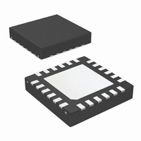
IC LED DRIVER PHOTO FLASH 24-LLP
Manufacturer
National Semiconductor
Series
PowerWise®r
Type
Photo Flash LEDr
Datasheet
1.LM2754SQNOPB.pdf
(11 pages)
Specifications of LM2754SQX/NOPB
Constant Current
Yes
Topology
Switched Capacitor (Charge Pump)
Number Of Outputs
4
Internal Driver
Yes
Type - Primary
Flash/Torch
Type - Secondary
White LED
Frequency
700kHz ~ 1.3MHz
Voltage - Supply
2.8 V ~ 5.5 V
Voltage - Output
4.7 V ~ 5.1 V
Mounting Type
Surface Mount
Package / Case
24-LLP
Operating Temperature
-40°C ~ 85°C
Current - Output / Channel
800mA
Internal Switch(s)
Yes
Efficiency
90%
For Use With
LM2754SQEV - BOARD EVALUATION LM2754SQ
Lead Free Status / RoHS Status
Lead free / RoHS Compliant
Other names
LM2754SQX
Available stocks
Company
Part Number
Manufacturer
Quantity
Price
Company:

Part Number:
LM2754SQX/NOPB
Manufacturer:
NS
Quantity:
7 708


V
I
V
V
R
I
I
f
V
V
I
I
Dx
Q
SD
SW
IH
IL
Symbol
SETx
HR
OUT
IH
IL
OUT
Absolute Maximum Ratings
If Military/Aerospace specified devices are required,
please contact the National Semiconductor Sales Office/
Distributors for availability and specifications.
Electrical Characteristics
Limits in standard typeface are for T
range (-40˚C to +125 ˚C). Unless otherwise noted, specifications apply to the LM2754 Typical Application Circuit (pg.1) with
V
Note 1: Absolute Maximum Ratings indicate limits beyond which damage to the component may occur. Operating Ratings are conditions under which operation of
the device is guaranteed. Operating Ratings do not imply guaranteed performance limits. For guaranteed performance limits and associated test conditions, see the
Electrical Characteristics tables.
Note 2: All voltages are with respect to the potential at the GND pin.
Note 3: Internal thermal shutdown circuitry protects the device from permanent damage. Thermal shutdown engages at T
120˚C (typ.).
Note 4: The Human-body model is a 100 pF capacitor discharged through a 1.5kΩ resistor into each pin.
Note 5: In applications where high power dissipation and/or poor package thermal resistance is present, the maximum ambient temperature may have to be
derated. Maximum ambient temperature (T
dissipation of the device in the application (P
following equation: T
Note 6: Junction-to-ambient thermal resistance (θ
standard JESD51-7. The test board is a 4 layer FR-4 board measuring 102mm x 76mm x 1.6mm. The 2 imbedded copper layers cover roughly the same area as
the board. Thickness of copper layers are 70µm/35µm/35µm/70µm (2oz/1oz/1oz/2oz). Thermal vias are placed between the die attach pad in the 1st copper layer
/I
V
EN, T/F, TX, SEL pins
Continuous Power Dissipation
(Note 3)
Junction Temperature
(T
Storage Temperature Range
Lead Temp. (Soldering, 5 sec.)
ESD Rating (Note 4)
(IN, INSW)
SETx
IN
J-MAX-ABS
Human Body Model
, V
OUT
I
LED Current to Set Current
Ratio (Note 11)
Current Sink Headroom
Voltage (Note 10)
Output Voltage
Output Impedance
Quiescent Supply Current
Shutdown Supply Current
Switching Frequency
Logic Input High
Logic Input Low
Logic Input High Current
(Note 9)
Logic Input Low Current
(Note 9)
= 3.6V, V
SETx
pins
)
Pin Voltage
A-MAX
Parameter
EN
= T
= 1.8V, V
J-MAX-OP
- (θ
T/F
JA
A-MAX
= 0V, V
D-MAX
x P
J
-0.3V to (V
= 25˚C, and limits in boldface type apply over the full operating junction temperature
D-MAX
JA
) is dependent on the maximum operation junction temperature (T
R
I
I
I
I
1x Mode, I
1.5x Mode, I
2x Mode, I
1x Mode
1.5x Mode
2x Mode
1x Mode, I
1.5x Mode, I
2x Mode, I
V
Input Pins: EN, T/F, TX, SEL
Input Pins: EN, T/F, TX, SEL
V
V
Dx
Dx
Dx
Dx
), and the junction-to ambient thermal resistance of the part/package in the application (θ
) is taken from a thermal modeling result, performed under the conditions and guidelines set forth in the JEDEC
EN
(EN, T/F, TX, SEL)
(EN, T/F, TX, SEL)
SETx
Internally Limited
TX
= 50mA to 100mA
= 200mA
= 200mA
= 50mA
-65˚C to 150˚C
).
= 0V
-0.3V to 6.0V
(Notes 2, 7)
= 0V, V
w/ 6.0V max
= 20kΩ
(Notes 1, 2)
IN
Dx
Dx
Dx
Dx
+ 0.3V)
Dx
Dx
150˚C
260˚C
= 0mA
= 0mA
= 0mA
= 0mA
SEL
2kV
= 0mA
= 0mA
Conditions
= 1.8V
= 0V
= 0V, C
3
IN
Operating Ratings
Thermal Information
= C
Input Voltage (V
Junction Temperature Range (T
Ambient Temperature Range (T
(Note 5)
Junction-to-Ambient Thermal Resistance,
LLP-24 Package (θ
1
= C
2
= 2.2µF, C
IN
)
−11.5%
JA
−3.5%
−7%
Min
OUT
0.7
1.2
)
(Note 6)
= 4.7µF. (Note 8)
J-MAX-OP
J
=150˚C (typ.) and disengages at T
(Notes 1, 2)
1.244
0.25
A
Typ
J
795
820
550
150
4.7
4.7
5.1
1.3
1.5
0.7
3.4
6.3
0.1
0.5
)
)
1
4
= 125
o
C), the maximum power
+11.5%
-40˚C to +125˚C
+3.5%
-40˚C to +85 ˚C
+7%
Max
JA
1.3
0.4
8
1
), as given by the
2.8V to 5.5V
www.national.com
42˚C/W
mA/mA
Units
MHz
mV
mA
µA
µA
µA
Ω
V
V
V
J
=
Related parts for LM2754SQX/NOPB
Image
Part Number
Description
Manufacturer
Datasheet
Request
R

Part Number:
Description:
IC,Laser Diode/LED Driver,LLCC,24PIN,PLASTIC
Manufacturer:
National Semiconductor

Part Number:
Description:
IC LED DRIVER PHOTO FLASH 24-LLP
Manufacturer:
National Semiconductor
Datasheet:
Part Number:
Description:
IC,Laser Diode/LED Driver,LLCC,24PIN,PLASTIC
Manufacturer:
National Semiconductor
Part Number:
Description:
National Semiconductor [8-Bit D/A Converter]
Manufacturer:
National Semiconductor
Datasheet:
Part Number:
Description:
National Semiconductor [Media Coprocessor]
Manufacturer:
National Semiconductor
Datasheet:
Part Number:
Description:
Digitally Controlled Tone and Volume Circuit with Stereo Audio Power Amplifier, Microphone Preamp Stage and National 3D Sound
Manufacturer:
National Semiconductor
Datasheet:
Part Number:
Description:
Digitally Controlled Tone and Volume Circuit with Stereo Audio Power Amplifier, Microphone Preamp Stage and National 3D Sound
Manufacturer:
National Semiconductor
Datasheet:
Part Number:
Description:
AC97 Rev 2 Codec with Sample Rate Conversion and National 3D Sound
Manufacturer:
National Semiconductor
Part Number:
Description:
Manufacturer:
National Semiconductor
Datasheet:
Part Number:
Description:
Manufacturer:
National Semiconductor
Datasheet:
Part Number:
Description:
General Purpose, Low Voltage, Low Power, Rail-to-Rail Output Operational Amplifiers
Manufacturer:
National Semiconductor
Datasheet:
Part Number:
Description:
8-bit 20 MSPS flash A/D converter.
Manufacturer:
National Semiconductor
Datasheet:
Part Number:
Description:
Low Noise Quad Operational Amplifier
Manufacturer:
National Semiconductor
Datasheet:
Part Number:
Description:
Quad Differential Line Receivers
Manufacturer:
National Semiconductor
Datasheet: