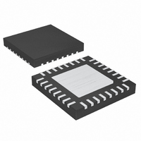
MAX8751ETJ+ Maxim Integrated Products, MAX8751ETJ+ Datasheet - Page 11

MAX8751ETJ+
Manufacturer Part Number
MAX8751ETJ+
Description
IC CNTRLR CCFL INV 32-TQFN
Manufacturer
Maxim Integrated Products
Type
CCFL Controllerr
Datasheet
1.MAX8751ETJT.pdf
(27 pages)
Specifications of MAX8751ETJ+
Frequency
30 ~ 80 kHz
Current - Supply
3.2mA
Voltage - Supply
6 V ~ 28 V
Operating Temperature
-40°C ~ 85°C
Package / Case
32-TQFN Exposed Pad
Lead Free Status / RoHS Status
Lead free / RoHS Compliant
Current - Output
-
Lead Free Status / Rohs Status
Details
PIN
18
19
20
21
22
23
24
25
26
27
28
29
30
31
32
—
PCOMP
PGND1
NAME
COMP
BST1
GND
ISEC
GH2
GH1
PAD
V
GL1
LX2
LX1
PS2
IFB
______________________________________________________________________________________
IN
CC
Gate-Driver Output for High-Side MOSFET NH2
Gate-Driver Return for GH2. LX2 is the input to the primary current-limit and zero-crossing
comparators. The controller senses the voltage across the low-side MOSFET NL2 (LX2 - GND) for
primary overcurrent condition and zero-crossing detection.
Supply Input. Input to the internal 5.3V linear regulator that powers the device. Bypass IN to GND with
a 0.1µF ceramic capacitor.
5.3V/20mA Linear Regulator Output. Supply voltage for the device including the low-side gate drivers
GL1 and GL2. Bypass V
Gate Driver Return for GH1. LX1 is the input to the primary current-limit and zero-crossing
comparators. The controller senses the voltage across the low-side MOSFET NL1 (LX1 - GND) for
primary overcurrent condition and zero-crossing detection.
Gate Driver Output for High-Side MOSFET NH1
High-Side Gate-Driver GH1 Supply Input. The MAX8751 includes an integrated boost diode. Connect
a 0.1µF capacitor between LX1 and BST1 to complete the bootstrap circuit.
Gate-Driver Output for Low-Side MOSFET NL1
Power Ground. PGND is the return for the GL1 gate driver.
System Ground
Compensation Node of the Phase-Lock Loop. Connect a 0.1µF capacitor between PCOMP and GND
to compensate the PLL.
Transconductance Error-Amplifier Output. A compensation capacitor of 0.01µF connected between
COMP and GND stabilizes the controller. The rise and fall time of the lamp-current envelope in DPWM
operation is also determined by the COMP capacitor.
Lamp Current-Feedback Input. The IFB sense signal is internally full-wave rectified. The average
value of the rectified signal is regulated to 790mV (typ) by controlling the on-time of the high-side
MOSFET. An open-lamp fault is generated if the IFB is continuously below 790mV (typ) for a period
set by TFLT. See the Lamp-Out Protection and Setting the Fault-Delay Time sections for details.
Phase-Shift Select Input for Slave. For details, see the Slave Operation (HFCK, LFCK, PSCK, DPWM)
section.
Transformer Secondary Current-Feedback Input. When the average voltage on ISEC exceeds the
internal overcurrent threshold, the controller turns on an internal current sink, discharging the COMP
capacitor. An RC current-sense network connected between the low-voltage end of the transformer
secondary and the ground allows setting the maximum secondary current during short-circuit fault.
Exposed Backside Pad. Connect PAD to GND.
Fixed-Frequency, Full-Bridge CCFL
CC
with a 1.0µF ceramic capacitor to GND.
DESCRIPTION
Inverter Controller
Pin Description (continued)
11


