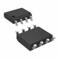
LM5100AM/NOPB National Semiconductor, LM5100AM/NOPB Datasheet - Page 5

LM5100AM/NOPB
Manufacturer Part Number
LM5100AM/NOPB
Description
IC DVR HALF-BRIDGE HV 8-SOIC
Manufacturer
National Semiconductor
Datasheet
1.LM5101CSDNOPB.pdf
(18 pages)
Specifications of LM5100AM/NOPB
Configuration
High and Low Side, Synchronous
Input Type
Non-Inverting
Delay Time
20ns
Current - Peak
3A
Number Of Configurations
1
Number Of Outputs
2
High Side Voltage - Max (bootstrap)
118V
Voltage - Supply
9 V ~ 14 V
Operating Temperature
-40°C ~ 125°C
Mounting Type
Surface Mount
Package / Case
8-SOIC (3.9mm Width)
Lead Free Status / RoHS Status
Lead free / RoHS Compliant
Other names
*LM5100AM
*LM5100AM/NOPB
LM5100AM
*LM5100AM/NOPB
LM5100AM
SUPPLY CURRENTS
I
I
I
I
I
I
INPUT PINS
V
V
V
V
R
UNDER VOLTAGE PROTECTION
V
V
V
V
BOOT STRAP DIODE
V
V
R
LO & HO GATE DRIVER
V
V
I
Symbol
DD
DDO
HB
HBO
HBS
HBSO
OHL
IL
IL
IHYS
IHYS
DDR
DDH
HBR
HBH
DL
DH
OL
OH
I
D
Absolute Maximum Ratings
If Military/Aerospace specified devices are required,
please contact the National Semiconductor Sales Office/
Distributors for availability and specifications.
Electrical Characteristics
Limits in standard type are for T
+125°C. Minimum and Maximum limits are guaranteed through test, design, or statistical correlation. Typical values represent the
most likely parametric norm at T
12V, V
VDD to VSS
HB to HS
LI or HI Input
LO Output
HO Output
HS to VSS
HB to VSS
SS
VDD Quiescent Current, LM5100A/B/C
VDD Quiescent Current, LM5101A/B/C
VDD Operating Current
Total HB Quiescent Current
Total HB Operating Current
HB to VSS Current, Quiescent
HB to VSS Current, Operating
Input Voltage Threshold LM5100A/B/C
Input Voltage Threshold LM5101A/B/C
Input Voltage Hysteresis LM5100A/B/C
Input Voltage Hysteresis LM5101A/B/C
Input Pulldown Resistance
VDD Rising Threshold
VDD Threshold Hysteresis
HB Rising Threshold
HB Threshold Hysteresis
Low-Current Forward Voltage
High-Current Forward Voltage
Dynamic Resistance LM5100A/B/C, LM5101A/B/
C
Low-Level Output Voltage LM5100A/LM5101A
Low-Level Output Voltage LM5100B/LM5101B
Low-Level Output Voltage LM5100C/LM5101C
High-Level Output Voltage LM5100A/LM5101A
High-Level Output Voltage LM5100B/LM5101B
High-Level Output Voltage LM5100C/LM5101C
Peak Pullup Current LM5100A/LM5101A
Peak Pullup Current LM5100B/LM5101B
Peak Pullup Current LM5100C/LM5101C
= V
(Note
HS
= 0V, No Load on LO or HO
6)
Parameter
J
J
= 25°C only; limits in boldface type apply over the junction temperature (T
= 25°C, and are provided for reference purposes only. Unless otherwise specified, V
V
HS
−0.3V to V
−0.3V to V
−0.3V to V
−0.3V to +18V
−0.3V to +18V
(Note
−5V to +100V
(Note
DD
DD
HB
4).
+0.3V
+0.3V
+0.3V
118V
1)
LI = HI = 0V
LI = HI = 0V
f = 500 kHz
LI = HI = 0V
f = 500 kHz
HS = HB = 100V
f = 500 kHz
Rising Edge
Rising Edge
I
I
I
I
I
V
V
HO, LO = 0V
VDD-HB
VDD-HB
VDD-HB
HO
HO
OH
OH
= I
= I
= VDD– LO or
= HB - HO
5
LO
LO
= 100 µA
= 100 mA
= 100 mA
Conditions
= 100 mA
= 100 mA
Recommended Operating
Conditions
VDD
HS
HB
HS Slew Rate
Junction Temperature
Junction Temperature
Storage Temperature Range
ESD Rating HBM
(Note
Min
100
4.5
1.3
6.0
5.7
2)
0.25
0.06
0.52
0.12
0.16
0.28
0.24
0.28
0.60
Typ
500
200
0.1
2.0
1.6
0.1
0.4
5.4
1.8
6.9
0.5
6.6
0.4
0.8
1.0
50
3
2
1
V
J
) range of -40°C to
HS
−55°C to +150°C
−40°C to +125°C
+8V to V
Max
0.85
1.65
0.25
0.65
0.45
0.60
1.10
400
0.2
0.4
0.2
6.3
2.3
7.4
7.1
0.4
+9V to +14V
−1V to 100V
10
3
3
1
www.national.com
DD
< 50 V/ns
+150°C
HS
= V
2 kV
+14V
Units
HB
mA
mA
mA
mA
mA
mV
mV
µA
kΩ
Ω
V
V
V
V
V
V
V
V
V
V
A
=


