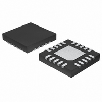
MAX4896ATP+ Maxim Integrated Products, MAX4896ATP+ Datasheet - Page 2

MAX4896ATP+
Manufacturer Part Number
MAX4896ATP+
Description
IC RELAY/LOAD DRVR 8CHAN 20-TQFN
Manufacturer
Maxim Integrated Products
Type
Relay/Load Driverr
Datasheet
1.MAX4896ETPT.pdf
(15 pages)
Specifications of MAX4896ATP+
Input Type
SPI
Number Of Outputs
8
On-state Resistance
3 Ohm
Current - Output / Channel
410mA
Current - Peak Output
960mA
Voltage - Supply
2.7 V ~ 5.5 V
Operating Temperature
-40°C ~ 125°C
Mounting Type
Surface Mount
Package / Case
20-TQFN Exposed Pad
Lead Free Status / RoHS Status
Lead free / RoHS Compliant
ABSOLUTE MAXIMUM RATINGS
(All voltages referenced to GND.)
V
OUT_ ....................................................................(-0.3V to +50V)
Continuous OUT_ Voltage ...................................................+50V
CS, SCLK, DIN, RESET, SPLD, PDCD ..................-0.3V to +7.0V
DOUT ............................................................-0.3V to (V
PGND to GND……………………………………..(-0.3V to +0.3V)
Continuous OUT_ Current, T
ELECTRICAL CHARACTERISTICS
(V
Stresses beyond those listed under “Absolute Maximum Ratings” may cause permanent damage to the device. These are stress ratings only, and functional
operation of the device at these or any other conditions beyond those indicated in the operational sections of the specifications is not implied. Exposure to
absolute maximum rating conditions for extended periods may affect device reliability.
Note 1: Maximum continuous current at a given temperature must be calculated such that the maximum continuous power
2
All Outputs On..................................................................210mA
Single Output On .............................................................420mA
Operating Voltage
Quiescent Current
Dynamic Average Supply
Current
Thermal Shutdown
Thermal-Shutdown Hysteresis
Power-On Reset
Power-On-Reset Hysteresis
DIGITAL INPUTS (SCLK, DIN, CS, RESET, PDCD, SPLD)
Input Logic-High Voltage
Input Logic-Low Voltage
Input Logic Hysteresis
Input Leakage Currents
Input Capacitance
RELAY OUTPUT DRIVERS (OUT1–OUT8)
OUT_ ON Resistance
I
S
OUT
S
......................................................................... -0.3V to +7.0V
= +2.7V to +5.5V, T
_______________________________________________________________________________________
Off-Leakage Current
dissipation for the package is not exceeded.
PARAMETER
Space-Saving, 8-Channel Relay/Load Driver
A
= -40°C to +125°C, unless otherwise noted. Typical values are at T
A
= +25°C (Note 1)
SYMBOL
T
V
V
I
I
T
V
R
SHDH
LEAK
LEAK
I
V
HYST
C
V
SHD
RSTH
V
CC
RST
I
ON
S
IH
IL
IN
S
I
0 or V
f
C
V
V
V
V
Input voltages = 0 or +5.5V
I
V
I
V
PDCD = high or RESET = low, all outputs
off
OUT
SCLK
V
OUT
OUT
S
S
S
S
S
S
OUT
S
= 2.7V to 3.6V
= 4.5V to 5.5V
= 2.7V to 3.6V
= 4.5V to 5.5V
= 2.7V
= 4.5V
falling
_ = 0, logic inputs =
= 50mA,
= 100mA,
S
= 10MHz, f
= 50pF, V
, RESET = low
S
+ 0.3V)
CONDITIONS
S
DIN
= 5.5V
= 0.5 x f
T
T
T
T
T
T
J
J
J
J
J
J
Continuous Power Dissipation (T
θ
Maximum Output Clamp Energy (E
Operating Temperature Range .........................-40°C to +125°C
Junction Temperature ......................................................+150°C
Storage Temperature Range .............................-65°C to +150°C
Lead Temperature (soldering, 10s) .................................+300°C
JA
= +25°C
= +125°C
= +150°C
= +25°C
= +125°C
= +150°C
V
V
20-Pin TQFN (derate 21.3mW/°C above +70°C) ......1702mW
S
S
................................................................................+47°C/W
CLK
= 3.6V
= 5V
,
MIN
A =
2.7
1.8
2.0
2.4
-1
-1
+25°C.) (Note 2)
A
+160
TYP
2.05
140
230
10
20
10
= +70°C)
OUT
5
5
3
_) ...........................30mJ
0.6
0.8
MAX
100
5.5
2.3
+1
+1
70
11
12
6
6
4
7
8
UNITS
mA
mV
mV
µA
µA
pF
µA
°C
°C
Ω
V
V
V
V


