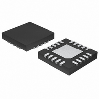
MAX4896ATP+ Maxim Integrated Products, MAX4896ATP+ Datasheet - Page 8

MAX4896ATP+
Manufacturer Part Number
MAX4896ATP+
Description
IC RELAY/LOAD DRVR 8CHAN 20-TQFN
Manufacturer
Maxim Integrated Products
Type
Relay/Load Driverr
Datasheet
1.MAX4896ETPT.pdf
(15 pages)
Specifications of MAX4896ATP+
Input Type
SPI
Number Of Outputs
8
On-state Resistance
3 Ohm
Current - Output / Channel
410mA
Current - Peak Output
960mA
Voltage - Supply
2.7 V ~ 5.5 V
Operating Temperature
-40°C ~ 125°C
Mounting Type
Surface Mount
Package / Case
20-TQFN Exposed Pad
Lead Free Status / RoHS Status
Lead free / RoHS Compliant
The MAX4896 is an 8-channel relay and load driver for
medium voltage applications up to 50V. The MAX4896
features built-in inductive kickback protection, drive for
latching/nonlatching, or dual-coil relays and an internal
register for detecting open-load and short-circuit faults.
Each independent open-drain output features a 3Ω on-
resistance and is guaranteed to sink 400mA at V
4.5V, and 100mA at V
The MAX4896 also incorporates a logic input (PDCD)
that allows the device to continue operating when an
overcurrent condition lasts longer than the 280µs (max)
fault delay time. A built-in overvoltage protection clamp
handles kickback voltage transients, which are com-
mon when driving inductive loads. Thermal-shutdown
circuitry shuts off all outputs (OUT_) when the junction
temperature exceeds +160°C.
The MAX4896 employs a reset input that allows the
user to turn off all outputs simultaneously with a single
control line.
The MAX4896 includes a 10MHz SPI-/QSPI-/MICROWIRE-
compatible serial interface. The serial interface is compat-
ible with TTL-/CMOS-logic voltage levels and operates
with a single +2.7V to +5.5V supply.
The serial interface consists of an 8-bit input shift regis-
ter, a parallel latch (output control register) controlled
by SCLK and CS, and an output status register contain-
ing diagnostics information. The input to the shift regis-
ter is an 8-bit word. Each data bit controls one of the
eight outputs, with the most significant bit (D7) corre-
sponding to OUT8, and the least significant bit (D0)
corresponding to OUT1 (see Table 1). When CS is low,
data at DIN is clocked into the shift register synchro-
nously with SCLK’s rising edge. Driving CS from low to
Figure 1. Serial Interface
8
SCLK
DIN
CS
_______________________________________________________________________________________
Space-Saving, 8-Channel Relay/Load Driver
OUTPUT CONTROL REGISTER (OUT)
OUTPUT STATUS REGISTER (OSR)
S
8-BIT SHIFT REGISTER
≤ 3.6V.
Detail Description
LATCHED ON CS:
LATCHED ON CS:
Serial Interface
DOUT
S
≥
high latches the data in the shift register to the output
control register.
DOUT is the output of the internal output status register
for diagnostics purposes (see Figure 2 and Tables 2
and 3). Status data for each channel is transferred to
the shift register at the falling edge of CS. The data bits
contained in the shift register are then transferred to the
DOUT output synchronously with SCLK’s falling edge.
While CS is low, the switches always remain in their
previous states. Drive CS high after 8 bits of data have
been shifted in to update the output state, and to further
inhibit data from entering the shift register. When CS is
high, transitions at DIN and SCLK have no effect on the
output, and the first input bit (D7) is present at DOUT.
If the number of data bits entered while CS is low is
greater or less than 8, the shift register contains only
the last 8 data bits, regardless of when they were
entered.
The 3-wire serial interface is compatible with SPI, QSPI,
and MICROWIRE standards. The latch that drives the
analog output stages is updated on the rising edge of
CS, regardless of SCLK’s state.
The MAX4896 contains an internal output status regis-
ter used for diagnostics information for each output
(see Tables 1, 2, and 3). When a fault condition is
detected at any channel for longer than the minimum
fault-filtering time (t
is latched into the corresponding position in the output
status register (see Table 2), and the FLAG asserts.
Status/diagnostics data for each channel in the output
status register is transferred to the output shift register
at the falling edge of CS. While CS is low, the diagnos-
tics bits are then transferred to DOUT synchronously
with SCLK’s falling edge. A rising edge at CS resets the
output status register data. During normal operation,
the output status bit is the same as the DIN bit (DO1 =
D1, DO2 = D2). When the MAX4896 is operating with a
fault condition, the output status bit is the inverse of the
DIN bit (DO1 = 0, D1 = 1).
D(FAULT)
Diagnostic Information
_min), the fault information


