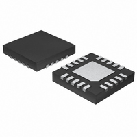
MAX4896ATP+ Maxim Integrated Products, MAX4896ATP+ Datasheet - Page 7

MAX4896ATP+
Manufacturer Part Number
MAX4896ATP+
Description
IC RELAY/LOAD DRVR 8CHAN 20-TQFN
Manufacturer
Maxim Integrated Products
Type
Relay/Load Driverr
Datasheet
1.MAX4896ETPT.pdf
(15 pages)
Specifications of MAX4896ATP+
Input Type
SPI
Number Of Outputs
8
On-state Resistance
3 Ohm
Current - Output / Channel
410mA
Current - Peak Output
960mA
Voltage - Supply
2.7 V ~ 5.5 V
Operating Temperature
-40°C ~ 125°C
Mounting Type
Surface Mount
Package / Case
20-TQFN Exposed Pad
Lead Free Status / RoHS Status
Lead free / RoHS Compliant
10, 16
PIN
11
12
13
14
15
17
18
19
20
—
1
2
3
4
5
6
7
8
9
Space-Saving, 8-Channel Relay/Load Driver
RESET
NAME
PGND
DOUT
PDCD
SCLK
OUT8
OUT7
OUT6
OUT5
OUT4
OUT3
OUT2
OUT1
FLAG
SPLD
GND
DIN
CS
_______________________________________________________________________________________
EP
V
S
Reset Input. Drive RESET low to clear all latches and registers (all outputs are turned off). All OUT
pulldown currents are disabled when RESET = low.
Chip Select Input. Drive CS low to select the device. When CS is low, data at DIN is clocked into the
8-bit shift register on SCLK’s rising edge. Drive CS from low to high to latch the data to the registers.
Serial Data Input
Serial Clock Input
Serial Data Output. DOUT is the output of the 8-bit shift register. This output can be used to daisy
chain multiple MAX4896s. The data at DOUT appears synchronous to SCLK’s falling edge.
Pulldown Current Disable. Drive PDCD high to disable OUT’s pulldown current source. Drive PDCD
low to enable OUT_ pulldown current source. PDCD must be low to detect an open-load fault.
Short-Protection Latch-Off Disable Input. Drive SPLD high to disable the built-in short-circuit
protection latch-off feature. When SPLD is low, an overloaded channel is turned off immediately. See
the Output Short-Circuit/Current-Limiting Protection section.
Open-Drain Output 8. Connect OUT8 to the low side of a relay coil. OUT8 is pulled to PGND when
activated and is otherwise high impedance.
Open-Drain Output 7. Connect OUT7 to the low side of a relay coil. OUT7 is pulled to PGND when
activated and is otherwise high impedance.
Power Ground. PGND is the ground return path for the output sinks. Connect PGND pins together
and to GND.
Open-Drain Output 6. Connect OUT6 to the low side of a relay coil. OUT6 is pulled to PGND when
activated and is otherwise high impedance.
Open-Drain Output 5. Connect OUT5 to the low side of a relay coil. OUT5 is pulled to PGND when
activated and is otherwise high impedance.
Ground
Open-Drain Output 4. Connect OUT4 to the low side of a relay coil. OUT4 is pulled to PGND when
activated and is otherwise high impedance.
Open-Drain Output 3. Connect OUT3 to the low side of a relay coil. OUT3 is pulled to PGND when
activated and is otherwise high impedance.
Open-Drain Output 2. Connect OUT2 to the low side of a relay coil. OUT2 is pulled to PGND when
activated and is otherwise high impedance.
Open-Drain Output 1. Connect OUT1 to the low side of a relay coil. OUT1 is pulled to PGND when
activated and is otherwise high impedance.
Input Supply Voltage. Bypass V
Open-Drain Fault Output. FLAG asserts low when a fault occurs at OUT1–OUT8.
Exposed Paddle. Internally connected to GND. Connect to a large PCB ground plane to improve
thermal dissipation. Enhances thermal conductivity; not intended as an electrical connection point.
S
to GND with a 0.1µF capacitor.
FUNCTION
Pin Description
7


