AMIS30623C623BRG ON Semiconductor, AMIS30623C623BRG Datasheet - Page 37
AMIS30623C623BRG
Manufacturer Part Number
AMIS30623C623BRG
Description
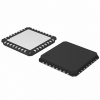
IC MOTOR DRIVER/CTLR 32-QFP
Manufacturer
ON Semiconductor
Datasheet
1.AMIS30623C6239RG.pdf
(61 pages)
Specifications of AMIS30623C623BRG
Applications
Stepper Motor Driver
Number Of Outputs
1
Current - Output
800mA
Voltage - Supply
6.5 V ~ 29 V
Operating Temperature
-40°C ~ 165°C
Mounting Type
Surface Mount
Package / Case
32-VSQFP
Mounting Style
SMD/SMT
Lead Free Status / RoHS Status
Lead free / RoHS Compliant
Voltage - Load
-
Lead Free Status / Rohs Status
Lead free / RoHS Compliant
Available stocks
Company
Part Number
Manufacturer
Quantity
Price
Company:

Part Number:
AMIS30623C623BRG
Manufacturer:
ON Semiconductor
Quantity:
1 850
Company:
Part Number:
AMIS30623C623BRG
Manufacturer:
ON Semiconductor
Quantity:
10 000


With:
Data error flag: (= Checksum error + StopBit error + Length
error)
Header error flag: (= Parity error + SynchField error)
Time out flag: The message frame is not fully completed
within the maximum length
Bit error flag: Difference in bit sent and bit monitored on the
LIN bus
A GetFullStatus frame will reset the error status register.
Physical Address of the Circuit
to discriminate this circuit from other ones on the LIN bus. This
address is coded on 7 bits, yielding the theoretical possibility
of 128 different circuits on the same bus. It is a combination of
4 OTP memory bits and of the 3 hardwired address bits (pins
HW[2:0]). However the maximum number of nodes in a LIN
network is also limited by the physical properties of the bus
line. It is recommended to limit the number of nodes in a LIN
network to not exceed 16. Otherwise the reduced network
impedance may prohibit a fault free communication under
worst case conditions. Every additional node lowers the
network impedance by approximately 3%.
NOTE:
to <ID5>, conform LIN1.3 specification. <ID6> = <ID0> ⊗
<ID1> ⊗ <ID2> ⊗ <ID4> (even parity) and <ID7> =
NOT(<ID1> ⊗ <ID3> ⊗ <ID4> ⊗ <ID5>) (odd parity).
NOTE:
following:
HW0 HW1 HW2
AD6 AD5 AD4 AD3 AD2 AD1 AD0 Physical address
ID0 ID1 ID2 ID3 ID4 ID5 ID6 ID7
0x3C
The circuit must be provided with a physical address in order
↑
<ID6> and <ID7> are used for parity check over <ID0>
The writing frames used with the AMIS−30623 are the
Type #1: General purpose 2 or 4 data bytes writing
ID
↑
Pins HW0 and HW1 are 5 V digital inputs, whereas pin
HW2 is compliant with a 12 V level, e.g. it can be
connected to Vbat or Gnd via a terminal of the PCB. For
SetPositionShort it is recommended to set HW0, HW1
and HW2 to ’1’.
Bit 7 of Data byte 1 must be at ‘1’ since the LIN specification requires that contents from 0x00 to 0x7F must be reserved for
broadcast messages (0x00 being for the “Sleep” message). See also LIN command Sleep
00
frame with a dynamically assigned identifier.
This type is dedicated to short writing actions
when the bus load can be an issue. They are
used to provide direct command to one
(<Broad> = ‘1’) or all the slave nodes
↑
Data Byte 1
Identifier Byte
AppCmd
PA3 PA2 PA1
1
Data Byte 2
command
PA0
physical address
OTP memory
Hardwired bits
Data Byte 3
phys. address
http://onsemi.com
Data Byte 1
Data Byte 4
37
LIN Frames
frames. A frame is composed of an 8−bit Identifier followed
by 2, 4 or 8 data−bytes and a checksum byte.
Note: The checksum is conform LIN1.3, classic checksum
calculation over only data bytes. (Checksum is an inverted
8−bit sum with carry over all data bytes.)
Writing frames will be used to:
•
•
•
•
Whereas reading frames will be used to:
•
•
•
Writing Frames
the slave nodes by means of a writing frame. According to
the LIN specification, identifiers are to be used to determine
a specific action. If a physical addressing is needed, then
some bits of the data field can be dedicated to this, as
illustrated in the example below.
within the data field in order to use less identifiers. One can
for example use the reserved identifier 0x3C and take
advantage of the 8 byte data field to provide a physical
address, a command and the needed parameters for the
action, as illustrated in the example below.
The LIN frames can be divided in writing and reading
The LIN master sends commands and/or information to
Another possibility is to determine the specific action
Program the OTP Memory;
Configure the component with the stepper−motor
parameters (current, speed, stepping−mode, etc.);
Provide set−point position for the stepper−motor;
Control the motion state machine.
Get the actual position of the stepper−motor;
Get status information such as error flags;
Verify the right programming and configuration of the
component.
Data Byte 5
(<Broad> = ‘0’). If <Broad> = ‘1’, the
physical address of the slave node is provided
by the 7 remaining bits of DATA2. DATA1 will
contain the command code (see Dynamic
assignment of Identifiers), while, if present,
DATA3 to DATA4 will contain the command
parameters, as shown below.
command parameters (e.g. position)
Data Byte 6
parameters
Data Byte 2
Data Byte 7
Data Byte 8
Related parts for AMIS30623C623BRG
Image
Part Number
Description
Manufacturer
Datasheet
Request
R

Part Number:
Description:
ON Semiconductor [VOLTAGE REGULATOR]
Manufacturer:
ON Semiconductor
Datasheet:
Part Number:
Description:
357-036-542-201 CARDEDGE 36POS DL .156 BLK LOPRO
Manufacturer:
ON Semiconductor
Datasheet:
Part Number:
Description:
357-036-542-201 CARDEDGE 36POS DL .156 BLK LOPRO
Manufacturer:
ON Semiconductor
Datasheet:
Part Number:
Description:
357-036-542-201 CARDEDGE 36POS DL .156 BLK LOPRO
Manufacturer:
ON Semiconductor
Datasheet:
Part Number:
Description:
357-036-542-201 CARDEDGE 36POS DL .156 BLK LOPRO
Manufacturer:
ON Semiconductor
Datasheet:
Part Number:
Description:
357-036-542-201 CARDEDGE 36POS DL .156 BLK LOPRO
Manufacturer:
ON Semiconductor
Datasheet:
Part Number:
Description:
357-036-542-201 CARDEDGE 36POS DL .156 BLK LOPRO
Manufacturer:
ON Semiconductor
Datasheet:
Part Number:
Description:
357-036-542-201 CARDEDGE 36POS DL .156 BLK LOPRO
Manufacturer:
ON Semiconductor
Datasheet:
Part Number:
Description:
357-036-542-201 CARDEDGE 36POS DL .156 BLK LOPRO
Manufacturer:
ON Semiconductor
Datasheet:
Part Number:
Description:
357-036-542-201 CARDEDGE 36POS DL .156 BLK LOPRO
Manufacturer:
ON Semiconductor
Datasheet:
Part Number:
Description:
357-036-542-201 CARDEDGE 36POS DL .156 BLK LOPRO
Manufacturer:
ON Semiconductor
Datasheet:
Part Number:
Description:
Manufacturer:
ON Semiconductor
Datasheet:
Part Number:
Description:
Manufacturer:
ON Semiconductor
Datasheet:
Part Number:
Description:
Manufacturer:
ON Semiconductor
Datasheet: