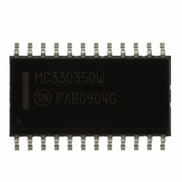
MC33035DWR2G ON Semiconductor, MC33035DWR2G Datasheet - Page 13

MC33035DWR2G
Manufacturer Part Number
MC33035DWR2G
Description
IC CTRLR MOTOR DC BRSHLSS 24SOIC
Manufacturer
ON Semiconductor
Type
Brushless DC Motor Controllerr
Datasheet
1.NCV33035DWR2G.pdf
(28 pages)
Specifications of MC33035DWR2G
Applications
DC Motor Controller, Brushless (BLDC)
Number Of Outputs
1
Current - Output
100mA
Voltage - Load
5.9 V ~ 6.5 V
Voltage - Supply
10 V ~ 30 V
Operating Temperature
-40°C ~ 85°C
Mounting Type
Surface Mount
Package / Case
24-SOIC (7.5mm Width)
Operating Supply Voltage
10 V to 30 V
Supply Current
20 mA
Mounting Style
SMD/SMT
Operating Current
20mA
Operating Temperature Classification
Industrial
Package Type
SOIC
Operating Supply Voltage (min)
10V
Operating Supply Voltage (max)
30V
Lead Free Status / RoHS Status
Lead free / RoHS Compliant
Other names
MC33035DWR2GOS
MC33035DWR2GOS
MC33035DWR2GOSTR
MC33035DWR2GOS
MC33035DWR2GOSTR
Available stocks
Company
Part Number
Manufacturer
Quantity
Price
Company:
Part Number:
MC33035DWR2G
Manufacturer:
FREESCALE
Quantity:
1 500
Part Number:
MC33035DWR2G
Manufacturer:
ON/安森美
Quantity:
20 000
t
Drive Outputs
collector NPN transistors capable of sinking 50 mA with a
minimum breakdown of 30 V. Interfacing into higher
voltage applications is easily accomplished with the circuits
shown in Figures 24 and 25.
21) are particularly suited for direct drive of N−Channel
MOSFETs or NPN bipolar transistors (Figures 26, 27, 28
and 29). Each output is capable of sourcing and sinking up
to 100 mA. Power for the bottom drives is supplied from V
(Pin 18). This separate supply input allows the designer
added flexibility in tailoring the drive voltage, independent
V
R
DLY
M
Reset
DLY
C
The three top drive outputs (Pins 1, 2, 24) are open
The three totem pole bottom drive outputs (Pins 19, 20,
DLY
[ R
[ R
22
17
18
4
5
6
3
8
7
DLY
DLY
Figure 23. Timed Delayed Latched
REF
25 μA
C
C
DLY
DLY
Over Current Shutdown
In
In
POS
DEC
UVLO
V
6.25 – (20 x 10 –6 R
1.4 – (20 x 10 –6 R
th
V
enable – (I
ref
– (I
IL
enable R
IL
enable R
DLY
DLY
DLY
)
)
DLY
)
MC33035, NCV33035
)
http://onsemi.com
14
2
1
24
21
20
C
13
of V
when driving power MOSFETs in systems where V
greater than 20 V so as to prevent rupture of the MOSFET
gates.
inverting input (Pin 15) must return on separate paths to the
central input source ground.
Thermal Shutdown
the IC in the event the maximum junction temperature is
exceeded. When activated, typically at 170°C, the IC acts as
though the Output Enable was grounded.
Decoder
Position
The control circuitry ground (Pin 16) and current sense
Internal thermal shutdown circuitry is provided to protect
Rotor
Transistor Q
high motor voltage, V
while V
CC
. A zener clamp should be connected to this input
Figure 24. High Voltage Interface with
M
is low.
1
is a common base stage used to level shift from V
NPN Power Transistors
M
. The collector diode is required if V
14
2
1
24
21
20
19
V
CC
Q
CC
1
Q
is present
CC
2
CC
to the
Q
Load
Q
3
4
V
is
M


