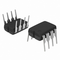
NCP1601BPG ON Semiconductor, NCP1601BPG Datasheet - Page 13

NCP1601BPG
Manufacturer Part Number
NCP1601BPG
Description
IC PFC CTRLR CRM/TRANSITION 8DIP
Manufacturer
ON Semiconductor
Datasheet
1.NCP1601APG.pdf
(19 pages)
Specifications of NCP1601BPG
Mode
Critical Conduction (CRM), Discontinuous (Transition)
Frequency - Switching
58kHz
Current - Startup
17µA
Voltage - Supply
9.6 V ~ 18 V
Operating Temperature
-40°C ~ 125°C
Mounting Type
Through Hole
Package / Case
8-DIP (0.300", 7.62mm)
Start-up Supply Current
17uA
Operating Supply Voltage (min)
-3V
Operating Supply Voltage (max)
18V
Operating Temp Range
-40C to 125C
Operating Temperature Classification
Automotive
Package Type
PDIP
Pin Count
8
Mounting
Through Hole
Switching Frequency
405 KHz
Maximum Operating Temperature
+ 125 C
Mounting Style
Through Hole
Minimum Operating Temperature
- 40 C
Lead Free Status / RoHS Status
Lead free / RoHS Compliant
Other names
NCP1601BPGOS
Available stocks
Company
Part Number
Manufacturer
Quantity
Price
Company:
Part Number:
NCP1601BPG
Manufacturer:
ON Semiconductor
Quantity:
1 500
Part Number:
NCP1601BPG
Manufacturer:
ON/安森美
Quantity:
20 000
voltage is higher based on the regulation block
characteristic in Figure 31. On the other hand, the V
in the low V
condition. In order to not over- - design the circuit in the
application, the V
very closed to V
almost 96% of the nominal value of R
condition while the output voltage is almost 100% of the
nominal value R
precision resistors in order to set the nominal V
and safety purpose.
voltage V
(300 kΩ typical) for the low- - pass filter in Figure 30. The
V
collected in the V
which is then compared to a ramp signal to generate the
MOSFET on time t
Overvoltage Protection (OVP)
reference current I
than 107% of its nominal value), the Drive Output pin
(Pin 7) of the device goes low for protection and the switch
of the V
automatically resumes operation when the output voltage
is lower than 107%.
corresponds to 225 mA 1.95 MΩ + 5 V = 443.75 V when
R
the worst case referring to Figure 11). Hence, it is generally
recommended to use 450 V rating output capacitor to allow
some design margin.
Undervoltage Protection (UVP)
reference current I
than 8% of its nominal value), the device is shut down and
consumes lower than 50 mA. In normal situation of boost
converter configuration, the output voltage V
higher than the input voltage V
I
It enables the NCP1601 to operate. Hence, UVP happens
when the output voltage is abnormally undervoltage, the
FB pin (Pin 1) is opened, or the FB pin (Pin 1) is manually
pulled low.
Current Sense
sense scheme in Figure 32. This scheme has the advantages
of: (1) the inrush current limitation by the resistor R
(2) the overcurrent protection and zero current detection
implemented in the same pin.
FB
control
FB
The feedback resistor R
The regulation block output V
When the feedback current I
The maximum OVP threshold is limited to 225 mA which
When the feedback current I
The device senses the inductor current I
is always higher than 8% of the reference current I
= 1.95 MΩ (1.8 MΩ + 150 kΩ) and V
and the time information of zero current are
control
control
ac
condition is much higher than the high V
processing circuit is kept off. The circuit
control(max)
FB
control
control
through an internal resistor R
ref
ref
1
I
for power factor correction.
(i.e., the output voltage V
(i.e., the output voltage V
ref
processing circuit to generate V
in the low V
in high V
FB
. It makes the output voltage be
consists of two or three high
FB
in
FB
reg
is higher than 107% of the
and the feedback current
is lower than 8% of the
ac
is connected to control
ac
condition.
condition is usually
FB
I
L
FB1
by the current
ref
out
out
out
out
in low V
= 5 V (for
is always
precisely
is higher
is lower
control
CS
http://onsemi.com
control
, and
ref
ton
ac
ac
.
13
negative voltage. This voltage is measured by a current I
flowing out of the CS pin (Pin 4). The CS pin has an offset
voltage V
zero inductor current I
current I
typical variation of offset voltage V
I
voltage at low current region creates lower the zero current
threshold for better accuracy. Based on Figure 32, (eq.13)
is derived.
Zero Current Detection (ZCD)
pin (Pin 4) sense current I
typical). The offset voltage of the CS pin in this condition
is V
The inductor current I
derived in (eq.14).
to make it reasonably close to zero, the settings of R
R
S
CS
Inductor current I
The device recognizes zero inductor current when the CS
It is obvious that the I
is shown in Figure 15. Higher the value of the offset
V
S(ZCD)
are crucial.
S(ZCD)
Figure 33. CS Pin Characteristic when I
R
R
L(OCP)
CS
I L(ZCD) =
S
S
. This offset voltage is studied in the setting of
(7.5 mV typical). It is illustrated in Figure 33.
Figure 32. Current Sensing
V
I
I
(i.e., overcurrent protection threshold). A
S
S
I
L
S(ZCD)
V S − R S I S = --R CS I L
L
R S I S(ZCD) − V S(ZCD)
passes through R
L(ZCD)
V
L(ZCD)
L(ZCD)
CS
+
- -
S
I
R
Ideal ZCD point
L
S
S
R
> R
is lower than I
S
NCP1601
Operating ZCD point
R CS
and the maximum inductor
= R
is not always zero. In order
S(ZCD)
at the ZCD condition is
S(ZCD)
Gnd
S
versus sense current
CS
S(ZCD)
and creates a
L
= 0
(14 mA
(eq.13)
(eq.14)
S
I
and
S
S


