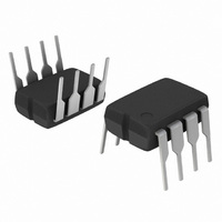
NCP1601BPG ON Semiconductor, NCP1601BPG Datasheet - Page 5

NCP1601BPG
Manufacturer Part Number
NCP1601BPG
Description
IC PFC CTRLR CRM/TRANSITION 8DIP
Manufacturer
ON Semiconductor
Datasheet
1.NCP1601APG.pdf
(19 pages)
Specifications of NCP1601BPG
Mode
Critical Conduction (CRM), Discontinuous (Transition)
Frequency - Switching
58kHz
Current - Startup
17µA
Voltage - Supply
9.6 V ~ 18 V
Operating Temperature
-40°C ~ 125°C
Mounting Type
Through Hole
Package / Case
8-DIP (0.300", 7.62mm)
Start-up Supply Current
17uA
Operating Supply Voltage (min)
-3V
Operating Supply Voltage (max)
18V
Operating Temp Range
-40C to 125C
Operating Temperature Classification
Automotive
Package Type
PDIP
Pin Count
8
Mounting
Through Hole
Switching Frequency
405 KHz
Maximum Operating Temperature
+ 125 C
Mounting Style
Through Hole
Minimum Operating Temperature
- 40 C
Lead Free Status / RoHS Status
Lead free / RoHS Compliant
Other names
NCP1601BPGOS
Available stocks
Company
Part Number
Manufacturer
Quantity
Price
Company:
Part Number:
NCP1601BPG
Manufacturer:
ON Semiconductor
Quantity:
1 500
Part Number:
NCP1601BPG
Manufacturer:
ON/安森美
Quantity:
20 000
OSCILLATOR
GATE DRIVE
FEEDBACK / OVERVOLTAGE PROTECTION / UNDERVOLTAGE PROTECTION
CURRENT SENSE
RAMP
THERMAL SHUTDOWN
ELECTRICAL CHARACTERISTICS
V
2. Comparator lower threshold is also the synchronization threshold.
3. Guaranteed by design.
Oscillator Frequency (Osc = 220 pF to GND)
Internal Capacitance of the Oscillator Pin
Maximum Oscillator Switching Frequency
Oscillator Discharge Current (Osc = 5.5 V)
Oscillator Charge Current (Osc = 3 V)
Comparator Lower Threshold (Osc = 220 pF to GND) (Note 3)
Comparator Upper Threshold (Osc = 220 pF to GND)
Synchronization Pulse Width for Detection
Synchronization Propagation Delay
Gate Drive Resistor
Output High and Draw 100 mA out of Drv Pin (I
Output Low and Insert 100 mA into Drv Pin (I
Gate Drive Rise Time from 1.5 V to 13.5 V (Drv = 1 nF to GND)
Gate Drive Fall Time from 13.5 V to 1.5 V (Drv = 1 nF to GND)
Reference Current
Regulation Block Ratio
V
Maximum Control Voltage (I
Feedback Pin Voltage (I
Overvoltage Protection Current Ratio
Overvoltage Protection Current
Undervoltage Protection Current Ratio
Current Sense Pin Offset Voltage (I
Overcurrent Protection Level
Current Sense Pin Offset Voltage at Overcurrent Level
Zero Current Detection Level
Current Sense Pin Offset Voltage at Zero Current Level
Zero Current Sense Resistor (R
Charging Current (Ramp = 0 V)
Maximum Power Resistance (R
Internal Clamping of Voltage V
Internal Capacitance of the Ramp Pin
Ramp Pin Sink Resistance (Osc = 0 V, Ramp = 1 mA sourcing)
Thermal Shutdown Threshold (Note 4)
Thermal Shutdown Hysteresis
control
control
= 100 nF, Ramp = 100 pF, Osc = 220 pF unless otherwise specified)
Pin Internal Resistor
FB
= 100 mA)
FB
Characteristic
ton
= 100 mA)
power
S(ZCD)
S
= 100 mA)
= V
= V
control(max)
(For typical values T
S(ZCD)
sink
source
= 100 mA)
/ I
S(ZCD)
/ I
= 100 mA)
ch
)
)
http://onsemi.com
J
= 25C. For min/max values, T
5
Pin
5
5
5
5
5
5
5
5
5
7
7
7
1
1
2
2
1
1
1
1
4
4
4
4
4
4
3
3
3
3
- -
- -
- -
V
I
I
I
C
t
control(max)
V
f
Symbol
C
V
OVP
UVP
V
R
V
regL
V
sync(min)
R
osc(max)
I
t
I
R
sync(d)
S(OCP)
S(ZCD)
ton(max)
ramp(int)
R
sync(H)
V
S(OCP)
osc(int)
I
sync(L)
I
S(ZCD)
S(ZCD)
R
R
control
T
f
odch
I
OVP
power
I
V
I
ramp
T
osc
och
FB1
ref
ch
OH
t
t
SD
OL
r
f
S
H
/ I
/ I
/ I
ref
ref
ref
J
= - -40C to +125C, V
0.95
Min
500
192
104
190
140
3.0
4.5
9.5
52
40
40
95
95
- -
- -
- -
5
2
- -
- -
- -
- -
- -
4
- -
0
9
0
- -
- -
- -
- -
- -
0.536
11.6
1.05
10.5
71.5
Typ
405
371
203
300
107
217
203
100
3.5
7.2
3.2
7.5
3.9
58
36
49
45
53
32
96
14
20
45
5
- -
3
8
4
- -
CC
= 15 V,
Max
1.15
11.5
208
225
210
105
4.0
5.5
64
60
60
20
18
97
15
20
19
20
1
- -
- -
- -
- -
- -
- -
- -
- -
- -
- -
- -
- -
- -
- -
- -
Unit
kHz
kHz
mV
mV
mV
kΩ
kΩ
kΩ
pF
mA
mA
mA
mA
mA
mA
mA
pF
C
C
ns
ns
ns
ns
%
%
%
V
V
Ω
Ω
V
V
V
Ω


