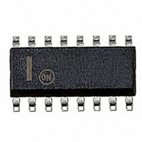
NCP1603D100R2G ON Semiconductor, NCP1603D100R2G Datasheet - Page 23

NCP1603D100R2G
Manufacturer Part Number
NCP1603D100R2G
Description
IC CTLR PFC/PWM COMBO 16-SOIC
Manufacturer
ON Semiconductor
Datasheet
1.NCP1603D100R2.pdf
(30 pages)
Specifications of NCP1603D100R2G
Mode
Critical Conduction (CRM), Discontinuous Conduction (DCM)
Frequency - Switching
58kHz
Current - Startup
17µA
Voltage - Supply
9 V ~ 18 V
Operating Temperature
-40°C ~ 125°C
Mounting Type
Surface Mount
Package / Case
16-SOIC (3.9mm Width)
Switching Frequency
405 KHz
Maximum Operating Temperature
+ 125 C
Mounting Style
SMD/SMT
Minimum Operating Temperature
- 40 C
Lead Free Status / RoHS Status
Lead free / RoHS Compliant
a 9.0 V ESD zener diode. The 3.9 V maximum limit of this
V
control voltage V
inductor current. The circuit in Figure 61 makes
Equations 9 and 10 where the value of resistor R
higher than the value of resistor R
V
obtained from Equations 3 through 10.
circuit output voltage (i.e., bulk voltage V
slowly varying signal. The bandwidth of V
additionally limited by inserting an external capacitor
C
internal 300 kW resistor and the capacitor C
low−pass filter that has a bandwidth f
It is generally recommended to limit the bandwidth below
20 Hz to achieve power factor correction. Typical value of
C
C
ton
control
control
control
The V
It is noted that V
In summary, the input impedance Z
Control voltage V
control
indirectly limits the maximum on time.
V
(V
is 0.1 mF.
to the V
control
control
Figure 61. V
ton
q V
V ton +
10
Z in +
C control u
V ton + V control for CRM
processing circuit generates V
control
control
control
ton
V in
I in
control
control
T V control
is always greater than or equal to
t 1 ) t 2
R
).
+
pin (Pin 10) in Figure 62. The
1
and time information of zero
2p300kW f control
C ramp V control
Processing Circuit
comes from the PFC boost
−
+
closed when zero current
C
2LI ch
1
R
1
2
for DCM
2
(R
control
1
in
>> R
in Equation 11 is
in Equation 12.
control
R
bulk
control
2
3
).
) that is a
1
ton
is much
create a
(eq. 10)
(eq. 12)
(eq. 11)
can be
http://onsemi.com
(eq. 9)
from
V
C
ton
3
23
60 Hz line frequency, the input impedance Z
varying or roughly constant. Then, the power factor
correction is achieved in DCM and CRM.
Maximum Power in PFC Section
Equations 13 and 14 when the circuit efficiency η is
obtained or assumed. The variable V
input voltage.
controls the amount of output power, input power, or input
impedance. The maximum value of the control voltage
V
called maximum power resistor R
defined in Equation 18 and restricted to have a maximum
±10% variation (i.e., 9.5 kW p R
defining the maximum power in an application.
(P
maximum input power P
The suffix ac stands for RMS value.
R power +
control
If the bandwidth of V
Input and output power (P
From Equations 13 and 14, control voltage V
It means that the maximum input and output power
in(max)
The maximum input current I
Regulation Block
V
I ac(max) +
96%
reg
Figure 62. V
is 1.05 V (i.e., V
P in +
P out + h P in +
and P
P in(max) +
P out(max) +
I
ref
V control(max)
I
ref
out(max)
V ac 2
P in(max)
Z in
I ch
I
FB1
V ac
control
+
V ac 2 C ramp R power
) are limited to ±10% variation.
hV ac 2 C ramp R power
control
control(max)
V ac 2 C ramp V control
in(max)
+
hV ac 2 C ramp V control
300k
+
V
Low−Pass Filtering
control
V acC ramp R power
100 mA
1.05 V
2 L
in
is much less than the 50 or
2LI ch
2 L
is also derived in (eq.14).
and P
power
10
2LI ch
= 1.05 V). A parameter
ac(max)
power
2 L
C
+ 10.5 kW
ac
control
out
stands for the RMS
(10.5 kW typical) is
) are derived in
p 11.5 kW) for
V
Processing
Circuit
to deliver the
control
in
is slowly
(eq. 13)
(eq. 14)
(eq. 15)
(eq. 16)
(eq. 17)
(eq. 18)
control


