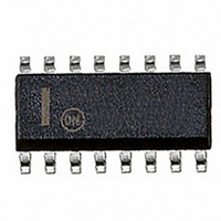
NCP1603D100R2G ON Semiconductor, NCP1603D100R2G Datasheet - Page 6

NCP1603D100R2G
Manufacturer Part Number
NCP1603D100R2G
Description
IC CTLR PFC/PWM COMBO 16-SOIC
Manufacturer
ON Semiconductor
Datasheet
1.NCP1603D100R2.pdf
(30 pages)
Specifications of NCP1603D100R2G
Mode
Critical Conduction (CRM), Discontinuous Conduction (DCM)
Frequency - Switching
58kHz
Current - Startup
17µA
Voltage - Supply
9 V ~ 18 V
Operating Temperature
-40°C ~ 125°C
Mounting Type
Surface Mount
Package / Case
16-SOIC (3.9mm Width)
Switching Frequency
405 KHz
Maximum Operating Temperature
+ 125 C
Mounting Style
SMD/SMT
Minimum Operating Temperature
- 40 C
Lead Free Status / RoHS Status
Lead free / RoHS Compliant
3. Consult factory for other frequency options.
4. Guaranteed by design.
ELECTRICAL CHARACTERISTICS
HV = 30 V, V
PWM OSCILLATOR
PWM GATE DRIVE
PWM CURRENT SENSE/OVERVOLTAGE PROTECTION
PWM STANDBY THRESHOLDS/FEEDBACK
AUXILIARY SUPPLY
PWM THERMAL SHUTDOWN
PWM STARTUP CURRENT SOURCE
Oscillation Frequency (T
Oscillation Frequency (T
Oscillation Frequency (T
Oscillator Modulation Swing, in Percentage of f
Oscillator Modulation Swing Period
Maximum Duty Ratio (V
Gate Drive Resistor
Output High (V
Output Low (Out2 = 1.0 V, V
Gate Drive Rise Time from 10% to 90% (Out2 = 1.0 nF to GND2)
Gate Drive Fall Time from 90% to 10% (Out2 = 1.0 nF to GND2)
Maximum Current Threshold (T
Maximum Current Threshold (T
Soft−Start Duration
Leading Edge Blacking Duration
Propagation Delay from CS Detected to Turn Out2 Off
Overvoltage Protection Threshold
Internal Compensation Ramp (Peak−to−Peak) (Note 4)
Internal Resistor to Ramp (Note 4)
Standby Thresholds
Feedback Voltage V
Feedback Voltage V
Validation Time for Leaving Standby
Validation Time for Recognize a Fault
Feedback Pin Sinking Capability (V
V
(V
Thermal Shutdown Threshold (Note 4)
Thermal Shutdown Hysteresis
High−Voltage Current Source
Startup (V
Startup (V
Leakage (V
Minimum Startup Voltage (V
aux
CC2
MOSFET Resistance
= 13 V, V
CC2
CC2
CC2
CC1
= V
= 0 V, HV = 30 V)
CC2
FB
= 13 V, HV = 700 V)
= 15 V, V
CC2(on)
= 2.0 V, V
Characteristic (PWM Section)
= 13 V, Out2 = 300 W to GND2)
FB2
FB2
CS2
to Start Standby
to Stop Standby
J
J
J
−0.2 V, V
control
= 25_C) (Note 3)
= 0_C to +125_C)
= −40_C to +125_C)
CC2
= 0 V, V
FB2
aux
J
J
= 20 mA Sinking)
= 100 nF, Ramp = 330 pF, Osc = 220 pF unless otherwise specified).
= 0 V)
= V
= −40_C to +125_C)
= 25_C)
FB2
FB2
CC2(on)
FB2
= 2.0 V, HV = 30 V)
= 0.75 V)
= 2.0 V)
(For typical values T
−0.2 V, I
osc2
HV
= 0.5 mA)
http://onsemi.com
J
= 25°C, for min/max values, T
6
Pin
13
13
13
16
16
−
−
−
−
3
−
3
−
3
3
3
2
2
2
2
1
−
−
T
V
V
Symbol
t
delay(CS)
stby−aux
R
start(min)
V
stby−out
R
V
D
R
V
T
f
I
R
t
t
I
I
I
I
T
osc2
Limit
t
LEB
comp
comp
fault
FB2
HV1
HV2
HV3
OH2
t
t
OVP
SD2
max
OL2
SS
stby
aux
−
−
r2
f2
H2
J
= −40°C to +125°C, V
0.991
0.96
Min
100
200
150
6.0
3.0
2.7
9.0
0.6
1.0
6.0
1.8
1.8
93
90
85
75
10
−
−
−
−
−
−
−
−
−
−
−
"6.4
1.043
12.3
0.75
1.25
Typ
11.7
100
200
125
125
235
165
5.0
7.5
2.5
3.0
2.3
3.2
4.4
80
40
15
90
18
25
30
20
−
−
−
CC2
= 13 V,
1.095
1.106
Max
107
350
180
270
110
110
3.3
0.9
1.5
4.2
5.6
85
25
18
36
23
80
23
−
−
−
−
−
−
−
−
−
−
Unit
kHz
mA
mA
ms
ms
kW
ms
ms
mA
mA
°C
°C
ns
ns
ns
ns
%
%
W
W
W
V
V
V
V
V
V


