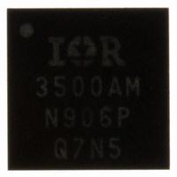
IR3500AMTRPBF International Rectifier, IR3500AMTRPBF Datasheet - Page 13

IR3500AMTRPBF
Manufacturer Part Number
IR3500AMTRPBF
Description
IC CTRL XPHASE3 VR11.0 32-MLPQ
Manufacturer
International Rectifier
Series
XPhase3™r
Datasheet
1.IR3500AMTRPBF.pdf
(48 pages)
Specifications of IR3500AMTRPBF
Applications
Processor
Current - Supply
6.5mA
Voltage - Supply
4.75 V ~ 7.5 V
Operating Temperature
0°C ~ 100°C
Mounting Type
Surface Mount
Package / Case
32-MLPQ
Package
32-Lead MLPQ
Circuit
X-Phase Control IC
Switch Freq (khz)
250kHz to 1.5MHz
Pbf
PbF Option Available
Lead Free Status / RoHS Status
Lead free / RoHS Compliant
Other names
IR3500AMTRPBFTR
IR3500A
Average Current Share Loop
Current sharing between phases of the converter is achieved by the average current share loop in each phase IC.
The output of the current sense amplifier is compared with average current at the share bus. If current in a phase is
smaller than the average current, the share adjust amplifier of the phase will pull down the starting point of the PWM
ramp thereby increasing its duty cycle and output current; if current in a phase is larger than the average current,
the share adjust amplifier of the phase will pull up the starting point of the PWM ramp thereby decreasing its duty
cycle and output current. The current share amplifier is internally compensated so that the crossover frequency of
the current share loop is much slower than that of the voltage loop and the two loops do not interact.
IR3500A THEORY OF OPERATION
Block Diagram
The Block diagram of the IR3500A is shown in Figure 8, and specific features are discussed in the following
sections.
VID Control
The AMD 6-bit VID, VR11 8-bit VID, and AMD Opteron 5-bit VID are shown in Tables 2 to 4 respectively, and are
selected by different connections of VIDSEL pin shown in Table 1. The VID pins require an external bias voltage
and should not be floated. The VID input comparators monitor the VID pins and control the Digital-to-Analog
Converter (DAC) whose output is sent to the VDAC buffer amplifier. The output of the buffer amplifier is the VDAC
pin. The VDAC voltage, input offsets of error amplifier and remote sense differential amplifier are post-package
trimmed to provide 0.5% system set-point accuracy. The actual VDAC voltage does not determine the system
accuracy, which has a wider tolerance. VIDs of less than 0.5V are not supported.
The IR3500A can accept changes in the VID code while operating and vary the DAC voltage accordingly. The slew
rate of the voltage at the VDAC pin can be adjusted by an external capacitor between VDAC pin and LGND pin. A
resistor connected in series with this capacitor is required to compensate the VDAC buffer amplifier. Digital VID
transitions result in a smooth analog transition of the VDAC voltage and converter output voltage minimizing inrush
currents in the input and output capacitors and overshoot of the output voltage.
Adaptive Voltage Positioning
Adaptive voltage positioning is needed to reduce the output voltage deviations during load transients and the power
dissipation of the load at heavy load. The circuitry related to voltage positioning is shown in Figure 9. The output
voltage is set by the reference voltage VSETPT at the positive input to the error amplifier. This reference voltage
can be programmed to have a constant DC offset bellow the VDAC by connecting RSETPT between VDAC and
VSETPT. The IVSETPT is controlled by the ROSC as shown in Figure 24.
The voltage at the VDRP pin is a buffered version of the share bus IIN and represents the sum of the DAC voltage
and the average inductor current of all the phases. The VDRP pin is connected to the FB pin through the resistor
R
. Since the error amplifier will force the loop to maintain FB to be equal to the VSETPT, an additional current
DRP
will flow into the FB pin equal to (VDRP-VSETPT) / R
. When the load current increases, the adaptive positioning
DRP
voltage increases accordingly. More current flows through the feedback resistor R
, and makes the output voltage
FB
lower proportional to the load current. The positioning voltage can be programmed by the resistor R
so that the
DRP
droop impedance produces the desired converter output impedance. The offset and slope of the converter output
impedance are referenced to and therefore independent of the VDAC voltage.
Inductor DCR Temperature Compensation
Page 13 of 48
July 28, 2009


