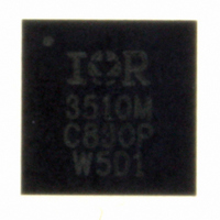
IR3510MTRPBF International Rectifier, IR3510MTRPBF Datasheet - Page 14

IR3510MTRPBF
Manufacturer Part Number
IR3510MTRPBF
Description
IC XPHASE CONTROL 32-MLPQ
Manufacturer
International Rectifier
Series
XPhase™r
Datasheet
1.IR3510MTRPBF.pdf
(36 pages)
Specifications of IR3510MTRPBF
Applications
Processor
Mounting Type
Surface Mount
Package / Case
32-MLPQ
Package
32-Lead MLPQ
Circuit
X-Phase Control IC
Pbf
PbF Option Available
Lead Free Status / RoHS Status
Lead free / RoHS Compliant
Current - Supply
-
Voltage - Supply
-
Operating Temperature
-
Other names
IR3510MTRPBFTR
Available stocks
Company
Part Number
Manufacturer
Quantity
Price
Part Number:
IR3510MTRPBF
Manufacturer:
IR
Quantity:
20 000
There is no unused or redundant silicon with the XPhase
controller that can be configured for 2, 3, or 4 phase operation. PCB Layout is easier since the 5 wire bus
eliminates the need for point−to−point wiring between the Control IC and each Phase. The critical gate drive and
current sense connections are short and local to the Phase ICs. This improves the PCB layout by lowering the
parasitic inductance of the gate drive circuits and reducing the noise of the current sense signal.
PWM Control Method
The PWM block diagram of the XPhase
with trailing edge modulation is used. Dual error amplifiers, outer loop voltage error amplifier and inner loop current
error amplifier, are used in the Control IC to control the PWM duty cycle. An external RC circuit connected to the
input voltage and ground is used to program the slope of the PWM ramp and to provide the feed−forward control at
each phase. The PWM ramp slope will change with the input voltage and automatically compensate for changes in
the input voltage. The input voltage can change due to variations in the silver box output voltage or due to drops in
the PCB related to changes in load current.
Frequency and Phase Timing Control
The oscillator is located in the Control IC and its frequency is programmable from 150 kHz to 1MHZ by an external
resistor. The output of the oscillator is a 50% duty cycle triangle waveform with peak and valley voltages of
approximately 4.8V and 0.9V. This signal is used to program both the switching frequency and phase timing of the
Phase ICs. The Phase IC is programmed by resistor divider RRAMP1 and RRAMP2 connected between the
VBIAS reference voltage and the Phase IC LGND pin. A comparator in the Phase ICs detects the crossing of the
oscillator waveform with the voltage generated by the resistor divider and triggers a clock pulse that starts the
PWM cycle. The peak and valley voltages track the VBIAS voltage reducing potential Phase IC timing errors.
Figure 4 shows the Phase timing for an 8 phase converter. Note that both slopes of the triangle waveform can be
used for synchronization by swapping the RAMP + and – pins.
Page 14 of 36
VPHASE4&5 (4.5V)
VPHASE3&6 (3.5V)
VPHASE2&7 (2.5V)
VPHASE1&8 (1.5V)
VVALLEY (1.00V)
VPEAK (5.0V)
CLK1
CLK2
CLK3
CLK4
CLK5
CLK6
CLK7
CLK8
50% RAMP
DUTY CYCLE
Figure 2 – 8 Phase Oscillator Waveforms
TM
architecture is also shown in Figure 1. Average current mode control
IR Confidential
SLOPE = 80mV / % DC
SLOPE = 1.6mV / ns @ 200kHz
SLOPE = 8.0mV / ns @ 1MHz
TM
architecture compared to others such as a 4 phase
May 18, 2009
IR3510


