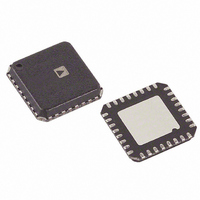
ADN8830ACPZ Analog Devices Inc, ADN8830ACPZ Datasheet - Page 18

ADN8830ACPZ
Manufacturer Part Number
ADN8830ACPZ
Description
IC CTRLR THERMO COOLER 32-LFCSP
Manufacturer
Analog Devices Inc
Datasheet
1.ADN8830ACPZ-REEL7.pdf
(24 pages)
Specifications of ADN8830ACPZ
Applications
Thermoelectric Cooler
Current - Supply
8mA
Voltage - Supply
3.3 V ~ 5 V
Operating Temperature
-40°C ~ 85°C
Mounting Type
Surface Mount
Package / Case
32-LFCSP
Ic Function
Thermoelectric Cooler Controller
Supply Voltage Range
3V To 5.5V
Operating Temperature Range
-40°C To +85°C
Digital Ic Case Style
LFCSP
No. Of Pins
32
Msl
MSL 1 - Unlimited
Lead Free Status / RoHS Status
Lead free / RoHS Compliant
Other names
015-0070
Q2376189
Q2376189
Available stocks
Company
Part Number
Manufacturer
Quantity
Price
Company:
Part Number:
ADN8830ACPZ
Manufacturer:
ADI
Quantity:
317
Part Number:
ADN8830ACPZ
Manufacturer:
ADI/亚德诺
Quantity:
20 000
ADN8830
The voltmeter to the TEC or output load should include the series
ammeter since the power delivered to the ammeter is considered part
of the total output power. However, the voltmeter measuring the
voltage delivered to the ADN8830 circuit should not include the
series ammeter from the power supply. This prevents a false supply
voltage power measurement since we are interested only in the
supply voltage power delivered to the ADN8830 circuit. Figures 16
and 17 show some efficiency measurements using the typical appli-
cation circuit shown in Figure 1.
Note that higher efficiency can be achieved using a lower supply
voltage or a slower clock frequency. This is due to the fact that the
dominant source of power dissipation at high clock frequencies is the
gate charge loss on the PWM transistors.
Layout Considerations
The two key considerations for laying out the board for the
ADN8830 are to minimize both the series resistance in the output
and the potential noise pickup in the precision input section. The
best way to accomplish both of these objectives is to divide the
layout into two sections, one for the output components and the
other for the remainder of the circuit. These sections should have
independent power supply and ground current paths that are each
connected together at a single point near the power supply. This is
used to minimize power supply and ground voltage bounce on the
more sensitive input stages to the ADN8830 caused by the switch-
ing of the PWM output. Such a layout technique is referred to as a
“star” ground and supply connection. Figure 18 shows a block dia-
gram of the concept.
100
100
80
60
40
20
80
60
40
20
0
0
0
0
Figure 17. Efficiency with f
Figure 16. Efficiency with f
V
SY
= 3V
500
500
V
SY
V
SY
= 5V
= 3V
V
SY
= 5V
I
I
TEC
TEC
1,000
1,000
(mA)
(mA)
CLK
CLK
1,500
1,500
= 200 kHz
= 1 MHz
2,000
2,000
–18–
The low noise power and ground are referred to as AVDD and
AGND, with the output supply and ground paths labeled PVDD
and PGND. These pins are labeled on the ADN8830 and should
be connected appropriately. Both sets of external FETs should be
connected to PVDD and PGND. All output filtering and PVDD
supply bypass capacitors should be connected to PGND.
All remaining connections to ground and power supply should be
done through AVDD and AGND. A 4-layer board layout is rec-
ommended for best performance with split power and ground
planes between the top and bottom layers. This provides the
lowest impedance for both supply and ground points. Setting the
ADN8830 above the AGND plane will reduce the potential noise
injection into the device. Figure 19 shows the top layer of the
layout used for the ADN8830 evaluation boards, highlighting the
power and ground split planes.
Proper supply voltage bypassing should also be taken into consid-
eration to minimize the ripple voltage on the power supply. A
minimum bypass capacitance of 10 F should be placed in close
proximity to each component connected to the power supply. This
includes Pins 8 and 20 on the ADN8830 and both external PMOS
transistors. An additional 0.1 F capacitor should be placed in
parallel to each 10 F capacitor to provide bypass for high fre-
quency noise. Using a large bulk capacitor, 100 F or greater, in
parallel with a low ESR capacitor where AVDD and PVDD con-
nect will further improve voltage supply ripple. This is covered in
more detail in the Power Supply Ripple section.
Figure 19. Top Layer Reference Layout for ADN8830
AVDD
Figure 18. Using Star Connections to Minimize
Noise Pickup from Switched Output
SENSITIVE
SECTION
NOISE
POWER SUPPLY
AGND
V
DD
GND
PGND
SECTION
OUTPUT
PVDD
LOAD
TEC
OR
REV. C


