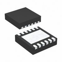
LTC2953IDD-2#PBF Linear Technology, LTC2953IDD-2#PBF Datasheet - Page 17

LTC2953IDD-2#PBF
Manufacturer Part Number
LTC2953IDD-2#PBF
Description
IC PB ON/OFF CONTROLLER 12DFN
Manufacturer
Linear Technology
Datasheet
1.LTC2953CDD-1PBF.pdf
(20 pages)
Specifications of LTC2953IDD-2#PBF
Applications
Push Button, On/Off Controller
Voltage - Supply
2.7 V ~ 27 V
Current - Supply
14µA
Operating Temperature
-40°C ~ 85°C
Mounting Type
Surface Mount
Package / Case
12-DFN
Ic Function
Push Button On/Off Controller With Voltage Monitoring
Supply Voltage Range
2.7V To 27V
Operating Temperature Range
-40°C To +85°C
Digital Ic Case Style
DFN
No. Of Pins
12
Svhc
No
Rohs Compliant
Yes
Lead Free Status / RoHS Status
Lead free / RoHS Compliant
Voltage - Input
-
Available stocks
Company
Part Number
Manufacturer
Quantity
Price
TYPICAL APPLICATIONS
Push Button Controlled μP Reset
The circuit of Figure 19 can be used to keep a μP in reset
for 200ms after the push button has enabled system power.
After system power has stabilized, the voltage monitor
input continues to monitor the supply at the load end.
ON/OFF
ON/OFF
3.3V
Figure 20. Push Button Controlled Supply Sequencing
3.3V
RST
VM
PB
Figure 19. Push Button Controlled μP Reset
PB
PB
LTC2953-2
LTC2953-2
V
IN
V
IN
R5
100k
RST
PFO
2953 F20
0.5V
VM
PFI
EN
RST
2953 F19
R5
100k
VM
EN
V
V
TH
TH
R9
100k
= 2.66V
= 2.01V
200ms
R9
100k
R3
866k
R2
200k
SHDN
DC/DC
R3
499k
R2
100k
V
#1
IN
TO LOAD
V
OUT
R11
510k
R15
604k
R16
200k
SHDN
V1
3.3V
DC/DC
V
#2
IN
V
OUT
V2
2.5V
Push Button Controlled Supply Sequencing
The circuit in Figure 20 uses the LTC2953-2 to sequence
3 supply rails. Power on sequencing begins by pressing
the push button for 32ms. This asserts the ⎯ E ⎯ N output low,
which turns on the V1 supply. 200ms after V1 reaches 80%
of its fi nal value (2.66V), the V2 supply is enabled. When
the V2 DC voltage reaches 80% of its fi nal value (2V), the
V3 supply is enabled. Note that there is no internal delay
from the ⎯ P ⎯ F ⎯ I input to the ⎯ P ⎯ F ⎯ O output and so V3 is enabled
at the same time V2 rises above 2V.
A power down supply sequence begins when any of these
inputs is asserted: ⎯ P ⎯ B , UVLO or ⎯ K ⎯ I ⎯ L ⎯ L . When ⎯ E ⎯ N pulls up
to V
is immediately disabled (there is no 200ms delay from VM
to ⎯ R ⎯ S ⎯ T during power down). When V2 decays to 2V, V3 is
immediately disabled. See Figure 21 timing diagram.
Figure 21. Push Button Controlled Supply Sequence Timing
PB
EN
V1
V2
V3
IN
V3
1.8V
, V1 disconnects fi rst. When V1 decays to 2.66V, V2
32ms
POWER ON
80%
200ms
80%
LTC2953
POWER OFF
80%
80%
17
2953 F21
2953f


