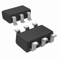
LM3880QMFE-1AB/NOPB National Semiconductor, LM3880QMFE-1AB/NOPB Datasheet

LM3880QMFE-1AB/NOPB
Specifications of LM3880QMFE-1AB/NOPB
Related parts for LM3880QMFE-1AB/NOPB
LM3880QMFE-1AB/NOPB Summary of contents
Page 1
... The output flags will follow a reverse sequence during power down to avoid latch condi- tions. EPROM capability allows every delay and sequence to be fully adjustable. Contact National Semiconductor if a non- standard configuration is required. Typical Application Circuit © 2008 National Semiconductor Corporation Features ■ ...
Page 2
Connection Diagram Pin Descriptions Pin # Name 1 VCC 2 GND FLAG3 5 FLAG2 6 FLAG1 Nomenclature Sequence Number See timing diagrams for more information www.national.com 20192602 Top View SOT23–6 Package ...
Page 3
... LM3880QMFE-1AC 60ms LM3880QMF-1AC 60ms LM3880QMFX-1AC 60ms LM3880QMFE-1AD 120ms LM3880QMF-1AD 120ms LM3880QMFX-1AD 120ms *Non-standard parts are available upon request. Please contact National Semiconductor for more information. **Automotive Grade (Q) product incorporates enhanced manufacturing and support processes for the automotive market, including defect detection methodologies ...
Page 4
... Absolute Maximum Ratings If Military/Aerospace specified devices are required, please contact the National Semiconductor Sales Office/ Distributors for availability and specifications. VCC EN, FLAG1, FLAG2, FLAG3 Max Flag 'ON' Current Storage Temperature Range Junction Temperature Lead Temperature (Soldering, 5 sec.) Minimum ESD Rating Electrical Characteristics apply over the full Operating Temperature Range (T test, design or statistical correlation ...
Page 5
Typical Performance Characteristics Quiescent Current vs VCC Enable Threshold vs Temperature Time Delay Ratio vs Temperature Quiescent Current vs Temperature (VCC = 3.3V) 20192604 Time Delay (30ms) vs VCC 20192606 Time Delay (30ms) vs Temperature 20192608 5 20192605 20192607 20192609 ...
Page 6
FLAG V vs VCC 100 kΩ) FLAG Block Diagram www.national.com FLAG Voltage vs Current 20192610 Block Diagram 6 20192611 20192612 ...
Page 7
Timing Diagrams (Sequence 1) All standard options use this sequence for output flags rise and fall order. Application Information OVERVIEW The LM3880 Power Sequencer provides an easy solution for sequencing multiple rails in a controlled manner. Six inde- pendent timers ...
Page 8
Cap Timing Using the internal pull-up current source to charge the exter- nal capacitor (C ) the enable pin delay can be calculated by EN the equation below: If the enable signal remains high for the entire power-up se- quence, ...
Page 9
... FLAG1 will always be first). How- ever, for some systems a different power down order could be required. To allow flexibility for this aspect in a design, the tity. Please contact National Semiconductor for more infor- mation. The variables that can be programmed include the six delay timers and the reverse sequence order ...
Page 10
Power Down Sequence Options 10 20192619 ...
Page 11
Physical Dimensions inches (millimeters) unless otherwise noted SOT23-6 Package NS Package Number MF06A 11 www.national.com ...
Page 12
... For more National Semiconductor product information and proven design tools, visit the following Web sites at: Products Amplifiers www.national.com/amplifiers Audio www.national.com/audio Clock Conditioners www.national.com/timing Data Converters www.national.com/adc Displays www.national.com/displays Ethernet www.national.com/ethernet Interface www.national.com/interface LVDS www.national.com/lvds Power Management www.national.com/power Switching Regulators www.national.com/switchers LDOs www ...


