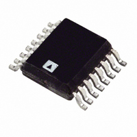
ADT7316ARQ-REEL7 Analog Devices Inc, ADT7316ARQ-REEL7 Datasheet - Page 5

ADT7316ARQ-REEL7
Manufacturer Part Number
ADT7316ARQ-REEL7
Description
IC SENSOR TEMP 12BIT DAC 16QSOP
Manufacturer
Analog Devices Inc
Datasheet
1.ADT7316ARQ.pdf
(44 pages)
Specifications of ADT7316ARQ-REEL7
Rohs Status
RoHS non-compliant
Function
Temp Monitoring System (Sensor)
Topology
ADC, Comparator, Multiplexer, Register Bank
Sensor Type
External & Internal
Sensing Temperature
-40°C ~ 120°C, External Sensor
Output Type
I²C™, MICROWIRE™, QSPI™, SMBus™, SPI™
Output Alarm
No
Output Fan
No
Voltage - Supply
2.7 V ~ 5.5 V
Operating Temperature
-40°C ~ 120°C
Mounting Type
Surface Mount
Package / Case
16-QSOP
For Use With
EVAL-ADT7316EBZ - BOARD EVAL FOR ADT7316
Lead Free Status / RoHS Status
Not Compliant
Parameter
DIGITAL OUTPUT
I
SPI TIMING CHARACTERISTICS
POWER REQUIREMENTS
1
2
3
4
5
6
7
8
9
10
11
12
13
2
gain error must be positive.
See the Terminology section.
DC specifications tested with the outputs unloaded.
Linearity is tested using a reduced code range: ADT7316 (Code 115 to 4095); ADT7317 (Code 28 to 1023); ADT7318 (Code 8 to 255).
A round robin is the continuous sequential measurement of the following three channels: V
Guaranteed by design and characterization, but not production tested.
For the amplifier output to reach its minimum voltage, the offset error must be negative. For the amplifier output to reach its maximum voltage, V
The SDA and SCL timing is measured with the input filters turned on to meet the fast-mode I
but has a negative effect on the EMC behavior of the part.
Guaranteed by design. Not tested in production.
The interface is also capable of handling the I
C TIMING CHARACTERISTICS
Output High Voltage, V
Output Low Voltage, V
Output High Current, I
Output Capacitance, C
INT/INT Output Saturation Voltage
Serial Clock Period, t
Data In Setup Time to SCL High, t
Data Out Stable After SCL Low, t
SDA Low Setup Time to SCL Low
SDA High Hold Time After SCL High
SDA and SCL Fall Time, t
SDA and SCL Rise Time, t
CS to SCLK Setup Time, t
SCLK High Pulse Width, t
SCLK Low Pulse Width, t
Data Access Time After SCLK Falling
Data Setup Time Prior to SCLK
Data Hold Time after SCLK Rising
CS to SCLK Hold Time, t
CS to DOUT High Impedance, t
V
V
I
I
Power Dissipation
Guaranteed by design and characterization, but not production tested.
All input signals are specified with tr = tf = 5 ns (10% to 90% of V
Measured with the load circuit of Figure 5.
I
DD
DD
DD
(Start Condition), t
(Stop Condition), t
Edge, t
Rising Edge, t
Edge, t
DD
DD
(Normal Mode)
(Power-Down Mode)
specification is valid for all DAC codes. Interface inactive. All DACs active. Load currents excluded.
Settling Time
4
6
12
1
5
13
4
5
1
OH
OUT
OL
OH
7
3
6
1
6
2
7, 8
10, 11
8
2
3
Min
2.4
2.5
50
0
50
50
0
50
50
20
0
0
2.7
2
C standard mode rise time specification of 1000 ns.
Typ
2.2
DD
) and timed from a voltage level of 1.6 V.
Max
0.4
1
50
0.8
300
300
35
40
5.5
50
3
3
10
10
33
10
Rev. B | Page 5 of 44
9
Unit
V
V
mA
pF
V
μs
ns
ns
ns
ns
ns
ns
ns
ns
ns
ns
ns
ns
ns
ns
V
ms
mA
mA
μA
μA
mW
μW
DD
2
C specification. Switching off the input filters improves the transfer rate,
, internal temperature, and external temperature.
Conditions/Comments
I
I
V
I
Fast-mode I
See
See
See
See
See
See
See
See
See
See
See
See
See
V
V
V
V
V
V
V
SOURCE
OL
OUT
OH
DD
DD
DD
DD
DD
DD
DD
ADT7316/ADT7317/ADT7318
= 3 mA.
= 5 V.
= 4 mA.
settles to within 10% of its final voltage level.
= 3.3 V, V
= 5 V, V
= 3.3 V, V
= 5 V, V
= 3.3 V, using normal mode.
= 3.3 V, using shutdown mode.
Figure 4
Figure 4
Figure 4
Figure 4
Figure 4
Figure 7
Figure 7
Figure 7
Figure 7
Figure 7
Figure 7
Figure 7
Figure 7
= I
SINK
IH
IH
= 200 μA.
2
C. See
.
.
.
.
.
.
.
.
.
.
.
.
.
IH
IH
= V
= V
= V
= V
DD
DD
DD
DD
, and V
, and V
Figure 4
, and V
, and V
IL
IL
= GND.
IL
= GND.
IL
.
= GND.
= GND.
REF
= V
DD
, offset plus


