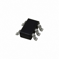
LM4130CIM5-2.5/NOPB National Semiconductor, LM4130CIM5-2.5/NOPB Datasheet - Page 4

LM4130CIM5-2.5/NOPB
Manufacturer Part Number
LM4130CIM5-2.5/NOPB
Description
IC REF PREC VOLT LDO SOT23-5
Manufacturer
National Semiconductor
Datasheet
1.LM4130AIM5-2.0.pdf
(11 pages)
Specifications of LM4130CIM5-2.5/NOPB
Reference Type
Series
Voltage - Output
2.5V
Tolerance
±0.1%
Temperature Coefficient
20ppm/°C
Voltage - Input
2.7 ~ 5.5 V
Number Of Channels
1
Current - Quiescent
75µA
Current - Output
20mA
Operating Temperature
-40°C ~ 85°C
Mounting Type
Surface Mount
Package / Case
SOT-23-5, SC-74A, SOT-25
Lead Free Status / RoHS Status
Lead free / RoHS Compliant
Current - Cathode
-
Other names
LM4130CIM5-2.5
LM4130CIM5-2.5TR
LM4130CIM5-2.5TR
www.national.com
V
TCV
(Note 6)
∆V
∆V
∆V
V
V
I
I
S
SC
REF
IN
N
LM4130-4.096
Electrical Characteristics
Unless otherwise specified V
boldface type apply over the operating temperature range.
Note 1: Absolute Maximum Ratings indicate limits beyond which damage to the device may occur. Operating Ratings indicate conditions for which the device is
intended to be functional, but do not guarantee specific performance limits. For guaranteed specifications and test conditions, see Electrical Characteristics. The
guaranteed specifications apply only for the test conditions listed. Some performance characteristics may degrade when the device is not operated under the listed
test conditions.
Note 2: Without PCB copper enhancements. The maximum power dissipation must be de-rated at elevated temperatures and is limited by T
junction temperature), θ
Note 3: The human body model is a 100 pF capacitor discharged through a 1.5 kΩ resistor into each pin. The machine model is a 200 pF capacitor discharged
directly into each pin.
Note 4: Typical numbers are at 25˚C and represent the most likely parametric norm.
Note 5: Limits are 100% production tested at 25˚C. Limits over the operating temperature range are guaranteed through correlation using Statistical Quality Control
(SQC) methods. The limits are used to calculate National’s Average Outgoing Quality Level (AOQL).
Note 6: Temperature coefficient is measured by the "Box" method; i.e., the maximum ∆V
Note 7: Long term stability is V
Note 8: Thermal hysteresis is defined as the change in +25˚C output voltage before and after cycling the device from −40˚C to 125˚C.
Note 9: Dropout voltage is defined as the minimum input to output differential at which the output voltage drops by 0.5% below the value measured with a 5V input.
= (T
REF
REF
REF
- V
Symbol
REF
JMAX
/∆V
/∆I
REF
/˚C
LOAD
− T
IN
A
)/θ
J-A
up to the value listed in the Absolute Maximum Ratings. θ
Output Voltage Initial
Accuracy
LM4130-4.096A
LM4130-4.096B
LM4130-4.096C
LM4130-4.096D
LM4130-4.096E
Temperature Coefficient
LM4130A, B
LM4130C, D
LM4130E
Line Regulation
Load Regulation
Long-Term Stability (Note
7)
Thermal Hysteresis
(Note 8)
Dropout Voltage
(Note 9)
Output Noise Voltage
Supply Current
Short Circuit Current
J-A
(junction to ambient thermal resistance) and T
REF
Parameter
@
CC
25˚C measured during 1000 hrs.
= 5.0V, I
LOAD
0˚C ≤ T
−40˚C ≤ T
I
V
0 mA ≤ I
1000 Hrs
−40˚C ≤ T
I
0.1 Hz to 10 Hz
LOAD
LOAD
= 0 T
REF
+ 500 mV ≤ V
A
= 100µA
= 10 mA
A
= 25˚C. Limits with standard typeface are for T
LOAD
Conditions
≤ +85˚C
A
A
A
(ambient temperature). The maximum power dissipation at any temperature is: PDiss
≤ +85˚C
≤ +125˚C
≤ 20 mA
J-A
4
for SOT23-5 package is 220˚C/W, T
IN
≤ 5.5V
REF
is divided by the maximum ∆T.
(Note 5)
Min
30
(Note 4)
JMAX
Typ
245
75
16
50
50
50
= 125˚C.
A
= 25˚C, and limits in
(Note 5)
±
Max
±
±
±
±
250
400
275
500
0.05
10
20
20
30
60
80
75
90
60
65
0.2
0.1
0.4
0.5
JMAX
ppm/mA
ppm/˚C
(maximum
ppm/V
Units
µV
ppm
mV
mA
mA
µA
%
PP
MAX


