LM5035CSQX/NOPB National Semiconductor, LM5035CSQX/NOPB Datasheet
LM5035CSQX/NOPB
Specifications of LM5035CSQX/NOPB


Related parts for LM5035CSQX/NOPB


LM5035CSQX/NOPB Summary of contents
Page 1
... The differences between LM5035, LM5035A, LM5035B, and LM5035C are summarized in Table Simplified Application Diagram © 2010 National Semiconductor Corporation LM5035C Features ■ 105V / 2A Half-Bridge Gate Drivers ■ ...
Page 2
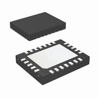
Connection Diagrams www.national.com 20-Lead TSSOP EP Top View LLP-24 Package Top View 30106803 2 30106802 ...
Page 3
Ordering Information Order Number Package Type LM5035CMH TSSOP-20EP LM5035CMHX TSSOP-20EP LM5035CSQ LLP-24 LM5035CSQX LLP-24 Pin Descriptions TSSOP LLP PIN Name PIN 1 23 RAMP Modulator ramp signal 2 24 UVLO Line Under-Voltage Lockout 3 2 OVP Line Over-Voltage Protection 4 ...
Page 4
TSSOP LLP PIN Name PIN Boost voltage for the HO driver Switch node High side gate drive output Low side gate drive output PGND Power Ground ...
Page 5
... Absolute Maximum Ratings If Military/Aerospace specified devices are required, please contact the National Semiconductor Sales Office/ Distributors for availability and specifications. VIN to GND HS to GND HB to GND VCC to GND RT, DLY to GND COMP Input Current Electrical Characteristics apply over full Operating Junction Temperature range. V 27.4kΩ ...
Page 6
Symbol Parameter Soft-Start (SS Pin) I Charging current in normal SS operation Charging current during a hiccup mode restart Soft-stop Current Sink Oscillator (RT Pin) F Frequency 1 (at HO, half oscillator SW1 frequency) F Frequency 2 (at HO, half ...
Page 7
Symbol Parameter Thermal Shutdown T Shutdown temperature SD Hysteresis Thermal Resistance θ Junction to ambient, 0 LFPM Air JA Flow θ Junction to Case (EP) Thermal JC resistance θ Junction to ambient, 0 LFM Air Flow LLP- ...
Page 8
Typical Performance Characteristics V and V VCC REF REF REF Oscillator Frequency vs Temperature www.national.com vs V VIN 30106805 30106807 30106809 VCC VCC 30106806 Frequency vs RT 30106808 Soft-Start Current vs Temperature 30106810 ...
Page 9
Effective Comp Input Impedance 30106811 SR "T1" Parameter vs Temperature 30106813 R vs Deadtime DLY SR "T2" Parameter vs Temperature 9 30106812 30106814 www.national.com ...
Page 10
Block Diagram www.national.com FIGURE 1. 10 30106804 ...
Page 11
Functional Description The LM5035C PWM controller contains all of the features necessary to implement half-bridge voltage-mode controlled power converters. The LM5035C provides two gate driver outputs to directly drive the primary side power MOSFETs and two signal level outputs to ...
Page 12
Cycle-by-Cycle Current Limit The CS pin is driven by a signal representative of the trans- former primary current. If the voltage sensed at CS pin ex- ceeds 0.25V, the current sense comparator terminates the output driver pulse. ...
Page 13
FIGURE 2. Current Limit Restart Circuit FIGURE 3. Current Limit Restart Timing 13 30106815 30106816 www.national.com ...
Page 14
Soft-Start The soft-start circuit allows the regulator to gradually reach a steady state operating point, thereby reducing start-up stress- es and current surges. When bias is supplied to the LM5035C, the SS pin capacitor is discharged by an internal MOSFET. ...
Page 15
If load transient response is slowed by the 10% margin, the R value can be increased. The system signal-to-noise will FF be slightly decreased by increasing R FF Oscillator, Sync ...
Page 16
Synchronous Rectifier Control Outputs (SR1 & SR2) Synchronous rectification (SR) of the transformer secondary provides higher efficiency, especially for low output voltage converters. The reduction of rectifier forward voltage drop (0.5V - 1.5V) to 10mV - 200mV V DS significantly ...
Page 17
Applications Information The following information is intended to provide guidelines for the power supply designer using the LM5035C. VIN The voltage applied to the VIN pin, which may be the same as the system voltage applied to the power transformer’s ...
Page 18
FIGURE 8. Current Sense Using Current Sense Transformer FIGURE 9. Current Sense Using Current Sense Resistor (R1) If the current sense resistor method is used, the over-current condition will only be sensed while LO is driving the low-side MOSFET. Over-current ...
Page 19
MOSFET. The capacitor should be large enough to supply the MOSFET gate charge (Qg) without dis- charging to the point where the drop in gate voltage affects the MOSFET value ten to twenty ...
Page 20
FIGURE 10. Basic UVLO Configuration FIGURE 11. Basic Over-Voltage Protection FIGURE 12. UVLO/OVP Divider 20 30106829 30106830 30106831 ...
Page 21
The impedance seen looking into the resistor divider from the UVLO and OVP pins determines the hysteresis level. UVLO and OVP enable and disable thresholds are calculated using Outputs disabled due to VIN falling below UVLO threshold Outputs enabled due ...
Page 22
R1 and Q1 are added reduce the sensitivity to low level currents in the opto-coupler. Using the values of Figure 14, the opto-coupler collector ...
Page 23
0.01 µ 363 µs. SS The time t2 provides a periodic cool-down time for the power converter in the event of a sustained overload or short circuit. This off time results in lower average ...
Page 24
Printed Circuit Board Layout The LM5035C Current Sense and PWM comparators are very fast, and respond to short duration noise pulses. The components at the CS, COMP, SS, OVP, UVLO, DLY and the RT pins should be as physically close ...
Page 25
25 www.national.com ...
Page 26
Physical Dimensions www.national.com inches (millimeters) unless otherwise noted Molded TSSOP-20 NS Package Number MXA20A 24-Lead LLP Package NS Package Number SQA24B 26 ...
Page 27
Notes 27 www.national.com ...
Page 28
... For more National Semiconductor product information and proven design tools, visit the following Web sites at: www.national.com Products Amplifiers www.national.com/amplifiers Audio www.national.com/audio Clock and Timing www.national.com/timing Data Converters www.national.com/adc Interface www.national.com/interface LVDS www.national.com/lvds Power Management www.national.com/power Switching Regulators www.national.com/switchers LDOs www.national.com/ldo LED Lighting www ...