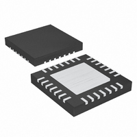
MAX5060ETI+T Maxim Integrated Products, MAX5060ETI+T Datasheet - Page 20

MAX5060ETI+T
Manufacturer Part Number
MAX5060ETI+T
Description
IC CNTRLR DC-DC 28-TQFN
Manufacturer
Maxim Integrated Products
Datasheet
1.MAX5061AUE.pdf
(31 pages)
Specifications of MAX5060ETI+T
Pwm Type
Current Mode
Number Of Outputs
1
Frequency - Max
1.5MHz
Duty Cycle
90%
Voltage - Supply
4.75 V ~ 28 V
Buck
Yes
Boost
No
Flyback
No
Inverting
No
Doubler
No
Divider
No
Cuk
No
Isolated
No
Operating Temperature
-40°C ~ 85°C
Package / Case
28-TQFN Exposed Pad
Frequency-max
1.5MHz
Output Voltage
0.6 V to 5.5 V
Output Current
30 A
Input Voltage
4.75 V to 5.5 V, 7 V to 28 V
Mounting Style
SMD/SMT
Maximum Operating Temperature
+ 85 C
Minimum Operating Temperature
- 40 C
Lead Free Status / RoHS Status
Lead free / RoHS Compliant
0.6V to 5.5V Output, Parallelable,
Average-Current-Mode DC-DC Controllers
where
RC2 = 10 , V
sense resistor. Note that the current limit of MAX5061 is
reduced by 3mV / R
The no-load output voltage depends on the R
V
CSN. The following equation assumes a 3mV bias volt-
age at CSP - CSN.
Powering new-generation processors requires new
techniques to reduce cost, size, and power dissipation.
Voltage positioning reduces the total number of output
capacitors to meet a given transient response require-
ment. Setting the no-load output voltage slightly higher
than the output voltage during nominally loaded condi-
tions allows a larger downward-voltage excursion when
the output current suddenly increases. Regulating at a
lower output voltage under a heavy load allows a larger
upward-voltage excursion when the output current sud-
denly decreases. Allowing a larger voltage-step excur-
sion reduces the required number of output capacitors
or allows for the use of higher ESR capacitors.
Voltage positioning may require the output to regulate
away from a center value. Define the center value as
the voltage where the output drops ( V
half the maximum output current (Figure 7).
Set the voltage-positioning window ( V
resistive feedback of the voltage-error amplifier (VEA).
Use the following equations to calculate the voltage-
positioning window (Figure 5):
MAX5060:
MAX5061:
R
VEA. G
is the current-sense resistor.
20
REF
IN
and R
______________________________________________________________________________________
V
(0.6V) and the fixed DC bias voltage at CSP -
OUT NL
C
I
L
is the current-loop transconductance and R
(
F
= peak-to-peak inductor current. Choose
V
are the input and feedback resistors of
)
OUT
CC
[(
V
Adaptive Voltage Positioning
OUT
V
= 5.1V, and R
R
REF
SENSE
G
L
I
C
OUT
G
C
.
V
I
OUT
REF
G
. 0 0289
c
R
R
R
R
F
F
IN
x R
S
x R
0 1
.
SENSE
F
)
H
R
H
R
R
H
OUT
L
OUT
R
]
is a current-
L
) using the
V
/2) at one
REF
H
, R
F
S
,
The high-side (DH) and low-side (DL) drivers drive the
gates of external n-channel MOSFETs (Figures 1 and 2).
The drivers’ 4A peak sink- and source-current capability
provides ample drive for the fast rise and fall times of the
switching MOSFETs. Faster rise and fall times result in
reduced cross-conduction losses. For modern CPU volt-
age-regulating module applications, where the duty
cycle is less than 50%, choose high-side MOSFETs (Q1)
with a moderate R
Choose low-side MOSFETs (Q2) with very low R
and moderate gate charge. Size the high-side and low-
side MOSFETs to handle the peak and RMS currents
during overload conditions.
The driver block also includes a logic circuit that provides
an adaptive nonoverlap time to prevent shoot-through
currents during transition. The typical nonoverlap time is
35ns between the high-side and low-side MOSFETs.
The MAX5060 uses V
MOSFET drivers. The low- and high-side drivers in the
MAX5061 are powered from V
derives its power through a bootstrap capacitor and V
supplies power internally to the low-side driver. Connect a
0.47µF low-ESR ceramic capacitor between BST and LX.
Connect a Schottky rectifier from BST to V
MAX5060, or to V
board area formed by the boost capacitor and rectifier.
Figure 7. Defining the Voltage-Positioning Window
V
V
V
CNTR
V
CNTR
V
OUT
OUT
CNTR
NO LOAD
/2
/2
-
+
MOSFET Gate Drivers (DH_, DL_)
CC
DS(ON)
DD
on the MAX5061. Reduce the PC
LOAD (A)
to power the low- and high-side
1/2 LOAD
and a very low gate charge.
CC
. The high-side driver
FULL LOAD
DD
DS(ON)
on the
BST
DD


