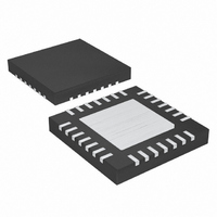
MAX5060ETI+T Maxim Integrated Products, MAX5060ETI+T Datasheet - Page 25

MAX5060ETI+T
Manufacturer Part Number
MAX5060ETI+T
Description
IC CNTRLR DC-DC 28-TQFN
Manufacturer
Maxim Integrated Products
Datasheet
1.MAX5061AUE.pdf
(31 pages)
Specifications of MAX5060ETI+T
Pwm Type
Current Mode
Number Of Outputs
1
Frequency - Max
1.5MHz
Duty Cycle
90%
Voltage - Supply
4.75 V ~ 28 V
Buck
Yes
Boost
No
Flyback
No
Inverting
No
Doubler
No
Divider
No
Cuk
No
Isolated
No
Operating Temperature
-40°C ~ 85°C
Package / Case
28-TQFN Exposed Pad
Frequency-max
1.5MHz
Output Voltage
0.6 V to 5.5 V
Output Current
30 A
Input Voltage
4.75 V to 5.5 V, 7 V to 28 V
Mounting Style
SMD/SMT
Maximum Operating Temperature
+ 85 C
Minimum Operating Temperature
- 40 C
Lead Free Status / RoHS Status
Lead free / RoHS Compliant
where D = V
(I
where C
tance.
For example, from the typical specifications in the
Applications Information section with V
high-side and low-side MOSFET RMS currents are 7.8A
and 18.5A, respectively for 20A. Ensure that the ther-
mal impedance of the MOSFET package keeps the
junction temperature at least +25°C below the absolute
maximum rating. Use the following equation to calcu-
late maximum junction temperature:
where
impedance and ambient temperature, respectively.
The discontinuous input-current waveform of the buck
converter causes large ripple currents in the input capac-
itor. The switching frequency, peak inductor current, and
the allowable peak-to-peak voltage ripple reflected back
to the source dictate the capacitance requirement.
Increasing switching frequency or paralleling multiple out-
of-phase converters lowers the peak-to-average current
ratio, yielding a lower input capacitance requirement for
the same load current.
The input ripple is comprised of V
capacitor discharge) and V
the capacitor). Use low-ESR ceramic capacitors with
high-ripple-current capability at the input. Assume the
contributions from the ESR and capacitor discharge are
equal to 30% and 70%, respectively. Calculate the input
capacitance and ESR required for a specified ripple
using the following equation:
OUT
2
+ I
I
RMS LO
C
JA
I
OSS
RMS HI
OSS
L
PD
/2).
and T
MOS LO
OUT
is the MOSFET drain-to-source capaci-
3
T
V
J
Average-Current-Mode DC-DC Controllers
A
/V
IN
= (PD
______________________________________________________________________________________
2
I DC I PK I
IN
are the junction-to-ambient thermal
2
I DC I PK I
2
, I
f
SW
DC
MOS
Q
G
2
= (I
2
ESR
x
1 4
.
OUT
V
JA
DC
DD
(caused by the ESR of
R
Input Capacitors
) + T
DC
DS ON
0.6V to 5.5V Output, Parallelable,
-
(
Q
I
PK
A
I
OUT
PK
I
f
(caused by the
SW
L
)
/2) and I
I
2
= 1.8V, the
1
D
RMS LO
3
3
D
PK
=
where I
For example, at V
itance are calculated for the input peak-to-peak ripple
of 100mV or less yielding an ESR and capacitance
value of 1.25m and 110µF.
The worst-case peak-to-peak and capacitor RMS ripple
current, the allowable peak-to-peak output ripple volt-
age, and the maximum deviation of the output voltage
during step loads determine the capacitance and the
ESR requirements for the output capacitors.
In buck converter design, the output-current waveform
is continuous and this reduces peak-to-peak ripple cur-
rent in the output capacitor equal to the inductor ripple
current. Calculate the capacitance, the ESR of the out-
put capacitor, and the RMS ripple current rating of the
output capacitor based on the following equations.
where V
butions due to ESR and the discharge of output capaci-
tor, respectively.
In the dynamic load environment, the allowable devia-
tion of output voltage during the fast transient load dic-
tates the output capacitance and ESR. The output
capacitors supply the load step until the controller
responds with a greater duty cycle. The response time
(t
the converter. The resistive drop across the capacitor
ESR and capacitor discharge causes a voltage drop
during a step load. Use a combination of SP polymer
and ceramic capacitors for better transient load and
ripple/noise performance.
RESPONSE
OUT
OESR
) depends on the closed-loop bandwidth of
is the output current of the converter.
ESR
C
OUT
and V
ESR
C
OUT
OUT
IN
IN
= 1.8V, the ESR and input capac-
8
I
OUT
OQ
V
I
V
OUT
Q
OESR
are the output-ripple contri-
I
V
L
V
OQ
ESR
D
I
L
Output Capacitors
f
1
SW
2
I
L
D
f
SW
25


