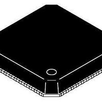
ADP3208DJCPZ-RL ON Semiconductor, ADP3208DJCPZ-RL Datasheet - Page 4

ADP3208DJCPZ-RL
Manufacturer Part Number
ADP3208DJCPZ-RL
Description
IC CTLR BUCK 7BIT 2PHASE 48LFCSP
Manufacturer
ON Semiconductor
Datasheet
1.ADP3208DJCPZ-RL.pdf
(37 pages)
Specifications of ADP3208DJCPZ-RL
Applications
Controller, Power Supplies for Next-Generation Intel Processors
Voltage - Input
3.3 ~ 22 V
Number Of Outputs
1
Voltage - Output
0.01 ~ 1.5 V
Operating Temperature
-10°C ~ 100°C
Mounting Type
Surface Mount
Package / Case
48-LFCSP
Output Voltage
10 mV
Output Current
40 A
Input Voltage
19 V
Supply Current
6 mA
Switching Frequency
300 KHz
Mounting Style
SMD/SMT
Maximum Operating Temperature
+ 100 C
Minimum Operating Temperature
- 10 C
Lead Free Status / RoHS Status
Lead free / RoHS Compliant
Available stocks
Company
Part Number
Manufacturer
Quantity
Price
Company:
Part Number:
ADP3208DJCPZ-RL
Manufacturer:
ON Semiconductor
Quantity:
10
Part Number:
ADP3208DJCPZ-RL
Manufacturer:
ON/安森美
Quantity:
20 000
PIN FUNCTION DESCRIPTIONS
Pin No
10
12
13
14
15
16
17
18
19
20
21
22
23
24
25
26
27
28
29
30
11
1
2
3
4
5
6
7
8
9
Mnemonic
VARFREQ
CSCOMP
IRPM/NC
PWRGD
CSSUM
PGND2
CLKEN
FBRTN
TTSNS
CSREF
DRVH2
PVCC2
DRVL2
COMP
RAMP
LLINE
ILIMN
VRTT
IMON
ILIMP
BST2
RPM
IREF
GND
SW2
EN
NC
NC
RT
FB
Enable Input. Driving this pin low shuts down the chip, disables the driver outputs, pulls PWRGD and VRTT
low, and pulls CLKEN high.
Power−Good Output. Open−drain output. A low logic state means that the output voltage is outside of the
VID DAC defined range.
Not Connected.
Clock Enable Output. Open−drain output. A low logic state enables the CPU internal PLL clock to lock to the
external clock.
Feedback Return Input/Output. This pin remotely senses the CPU core voltage. It is also used as the ground
return for the VID DAC and the voltage error amplifier blocks.
Voltage Error Amplifier Feedback Input. The inverting input of the voltage error amplifier.
Voltage Error Amplifier Output and Frequency Compensation Point.
Not Connected.
RPM Mode Timing Control Input. A resistor between this pin or RPM pin to ground sets the RPM mode
turn−on threshold voltage. If a resistor is connected between this pin to ground, RPM pin must remain
floating and not connected.
Variable Frequency Enable Input. A high logic state enables the PWM clock frequency to vary with VID code.
Voltage Regulator Thermal Throttling Output. Logic high state indicates that the voltage regulator
temperature at the remote sensing point exceeded a set alarm threshold level.
Thermal Throttling Sense and Crowbar Disable Input. A resistor divider where the upper resistor is
connected to VCC, the lower resistor (NTC thermistor) is connected to GND, and the center point is
connected to this pin and acts as a temperature sensor half bridge. Connecting TTSNS to GND disables the
thermal throttling function and disables the crowbar, or Overvoltage Protection (OVP), feature of the chip.
Current Monitor Output. This pin sources a current proportional to the output load current. A resistor to
FBRTN sets the current monitor gain.
RPM Mode Timing Control Input. A resistor between this pin or IRPM pin to ground sets the RPM mode
turn−on threshold voltage. If a resistor is connected between this pin to ground, IRPM pin must remain
floating.
This pin sets the internal bias currents. A 80 kW resistor is connected from this pin to ground.
Load Line Programming Input. The center point of a resistor divider connected between CSREF and
CSCOMP can be tied to this pin to set the load line slope.
Current Sense Amplifier Output and Frequency Compensation Point.
Current Sense Reference Input. This pin must be connected to the common point of the output inductors.
The node is shorted to GND through an internal switch when the chip is disabled to provide soft stop
transient control of the converter output voltage.
Current Sense Summing Input. External resistors from each switch node to this pin sum the inductor currents
to provide total current information.
PWM Ramp Slope Setting Input. An external resistor from the converter input voltage node to this pin sets
the slope of the internal PWM stabilizing ramp used for phase−current balancing.
Current Limit Set. An external resistor from ILIMN to ILIMP sets the current limit threshold of the converter.
Current Limit Set. An external resistor from ILIMN to ILIMP sets the current limit threshold of the converter.
PWM Oscillator Frequency Setting Input. An external resistor from this pin to GND sets the PWM oscillator
frequency.
Analog and Digital Signal Ground.
High−Side Bootstrap Supply for Phase 2. A capacitor from this pin to SW2 holds the bootstrapped voltage
while the high−side MOSFET is on.
High−Side Gate Drive Output for Phase 2.
Current Balance Input for Phase 2 and Current Return for High−Side Gate Drive.
Power Supply Input/Output of Low−Side Gate Driver for Phase 2.
Low−Side Gate Drive Output for Phase 2.
Low−Side Driver Power Ground for Phase 2.
http://onsemi.com
4
Description


