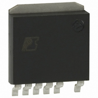
DPA423SN Power Integrations, DPA423SN Datasheet - Page 17

DPA423SN
Manufacturer Part Number
DPA423SN
Description
IC CONV DC-DC DPA SWITCH SPAK
Manufacturer
Power Integrations
Series
DPA-Switch®r
Specifications of DPA423SN
Applications
Converter, Power Over Ethernet and Telecom Applications
Voltage - Input
16 ~ 75 V
Number Of Outputs
1
Voltage - Output
220V
Operating Temperature
-40°C ~ 125°C
Mounting Type
Surface Mount
Package / Case
SPak (5 leads + Tab)
Mounting Style
SMD/SMT
For Use With
596-1195 - KIT REF DES DPA 6.6W DC-DC CONV
Lead Free Status / RoHS Status
Lead free / RoHS Compliant
Available stocks
Company
Part Number
Manufacturer
Quantity
Price
Company:
Part Number:
DPA423SN
Manufacturer:
POWER
Quantity:
15 000
Part Number:
DPA423SN
Manufacturer:
POWER
Quantity:
20 000
Company:
Part Number:
DPA423SN-TL
Manufacturer:
IDT
Quantity:
200
Part Number:
DPA423SN-TL
Manufacturer:
POWER
Quantity:
20 000
board material is used (such as FR4), providing copper areas on
both sides of the board and using thicker copper will improve
heat sinking.
If an aluminum clad board is used, then shielding of switching
nodes is recommended. This consists of an area of copper placed
directly underneath switching nodes such as the drain node
and output diode to provide an electrostatic shield to prevent
coupling to the aluminum substrate. These areas are connected
to input negative in the case of the primary and output return
for secondary. This reduces the amount of capacitive coupling
into the insulated aluminum substrate that can then appear on
the output as ripple and high frequency noise.
Quick Design Checklist
As with any power supply design, all DPA-Switch designs
should be verified on the bench to make sure that component
specifications limits are not exceeded under worst case
conditions. The following minimum set of tests for DPA-Switch
forward converters is strongly recommended:
Figure 13. Layout Considerations for DPA-Switch Using R Package.
TOP VIEW
+
-
V
Solder Side
Component Side
Maximize hatched copper area for optimum heat sinking
Via between board layers
DPA-Switch
V
V
C
D
X
S
L
V
coupler
Opto-
Transformer
1. Maximum drain voltage – Verify that peak drain-to-source
2. Transformer reset margin – Drain voltage should also be
3. Maximum drain current – At maximum ambient temperature,
voltage does not exceed minimum BV
voltage and maximum overload output power. It is normal,
however, to have additional margin of approximately 25 V
below BV
unit-to-unit variations. Maximum overload output power
occurs when the output is loaded to a level just before the
power supply goes into auto-restart (loss of regulation).
checked at highest input voltage with a severe load step
(50% to 100%) to verify adequate transformer reset margin.
This test slews the duty cycle at high input voltage, placing
the most demand on the transformer reset circuit.
maximum input voltage and maximum output load, verify
drain current waveforms at start-up for any signs of
transformer or output inductor saturation and excessive
leading edge current spikes. DPA-Switch has a leading edge
blanking time of 100 ns to prevent premature termination
of the cycle. Verify that the leading edge current spike does
not extend beyond the blanking period.
V
DSS
to allow for other power supply component
+
(Coupled)
-
Output
Diode
Inductor
DSS
Out
DC
AN-31
at highest input
PI-2883-060602
7/04
C
17


