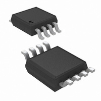
LM3488MM/NOPB National Semiconductor, LM3488MM/NOPB Datasheet

LM3488MM/NOPB
Specifications of LM3488MM/NOPB
LM3488MM
LM3488MMTR
Available stocks
Related parts for LM3488MM/NOPB
LM3488MM/NOPB Summary of contents
Page 1
... Power saving shutdown mode reduces the total supply current to 5µA and allows power supply sequencing. Internal soft-start limits the inrush current at start-up. Typical Application Circuit © 2010 National Semiconductor Corporation LM3488/LM3488Q Key Specifications ■ Wide supply voltage range of 2.97V to 40V ■ ...
Page 2
Connection Diagram Package Marking and Ordering Information Order Number Package Type LM3488MM LM3488MMX MSOP-8 LM3488QMM LM3488QMMX *Automotive Grade (Q) product incorporates enhanced manufacturing and support processes for the automotive market, including defect detection methodologies. Reliability qualification is compliant with the ...
Page 3
... Absolute Maximum Ratings If Military/Aerospace specified devices are required, please contact the National Semiconductor Sales Office/ Distributors for availability and specifications. Input Voltage FB Pin Voltage FA/SYNC/SD Pin Voltage Peak Driver Output Current (<10µs) Power Dissipation Storage Temperature Range Junction Temperature ESD Susceptibilty ...
Page 4
Symbol Parameter V Internal Compensation Ramp SL Voltage V ratio SENSE V Output Over-voltage OVP Protection (with respect to feedback voltage) (Note V Output Over-Voltage OVP(HYS) Protection Hysteresis(Note Gm Error Ampifier Transconductance A Error Amplifier Voltage ...
Page 5
Note 1: Absolute Maximum Ratings are limits beyond which damage to the device may occur. Operating Ratings are conditions under which operation of the device is intended to be functional. For guaranteed specifications and test conditions, see the Electrical Characteristics. ...
Page 6
Frequency vs Temperature Current Sense Threshold vs Input Voltage Efficiency vs Load Current (3.3V In and 12V Out) www.national.com Drive Voltage vs Input Voltage 10138854 COMP Pin Voltage vs Load Current 10138845 Efficiency vs Load Current (5V In and 12V ...
Page 7
Efficiency vs Load Current (9V In and 12V Out) Error Amplifier Gain COMP Pin Source Current vs Temperature Efficiency vs Load Current (3.3V In and 5V Out) 10138860 Error Amplifier Phase 10138855 Short Circuit Protection vs Input Voltage 10138836 7 ...
Page 8
Compensation Ramp vs Compensation Resistor Current Sense Voltage vs Duty Cycle www.national.com Shutdown Threshold Hysteresis vs Temperature 10138851 10138852 8 10138846 ...
Page 9
Functional Block Diagram Functional Description The LM3488 uses a fixed frequency, Pulse Width Modulated (PWM), current mode control architecture typical appli- cation circuit, the peak current through the external MOSFET is sensed through an external sense resistor. The ...
Page 10
SLOPE COMPENSATION RAMP The LM3488 uses a current mode control scheme. The main advantages of current mode control are inherent cycle-by-cy- cle current limit for the switch, and simpler control loop char- acteristics also easy to parallel power ...
Page 11
FIGURE 3. Compensation Ramp Avoids Sub-Harmonic Oscillation The compensation ramp has been added internally in LM3488. The slope of this compensation ramp has been se- lected to satisfy most of the applications. The slope of the internal compensation ramp depends ...
Page 12
FIGURE 5. ΔV SL FREQUENCY ADJUST/SYNCHRONIZATION/SHUTDOWN The switching frequency of LM3488 can be adjusted between 100kHz and 1MHz using a single external resistor. This re- sistor must be connected between FA/SYNC/SD pin and ground, as shown in Figure 6. Please ...
Page 13
FIGURE 8. Shutdown Operation in Frequency Adjust Mode FIGURE 9. Shutdown Operation in Synchronization Mode SHORT-CIRCUIT PROTECTION When the voltage across the sense resistor (measured on I Pin) exceeds 350mV, short-circuit current limit gets acti- SEN FIGURE 7. Frequency Synchronization ...
Page 14
Typical Applications The LM3488 may be operated in either continuous or discon- tinuous conduction mode. The following applications are de- signed for continuous conduction operation. This mode of operation has higher efficiency and lower EMI characteristics than the discontinuous mode. ...
Page 15
FIGURE 11. A. Inductor Current B. Diode Current If V (t) is constant, di (t)/dt must be constant. Hence, for given input voltage and output voltage, the current in the in- ductor changes at a constant rate. ...
Page 16
If Δi er than I , the inductor current will stay above zero and the L converter will operate in continuous conduction mode. All the analysis in this datasheet assumes operation in continuous conduction ...
Page 17
SETTING THE CURRENT LIMIT The maximum amount of current that can be delivered to the load is set by the sense resistor, R SEN when the voltage that is generated across the sense resistor equals the current sense threshold voltage, ...
Page 18
On-resistance, R (ON Total gate charge Reverse transfer capacitance Maximum drain to source voltage, V The off-state voltage of the MOSFET is approximately equal to the output voltage the MOSFET ...
Page 19
In the above equation the on-state voltage of the MOS- Q FET, Q, and V is the forward voltage drop of the diode. DIODE POWER MOSFET SELECTION As in boost converter, the parameters governing the selection of the ...
Page 20
I must be lower than the maximum current rating set by L1PK the current sense resistor. The value of L1 can be increased above the minimum rec- ommended to reduce input ripple and output ripple. However, once D is less ...
Page 21
Output Capacitor Selection The ESR and ESL of the output capacitor directly control the output ripple. Use low capacitors with low ESR and ESL at the output for high efficiency and low ripple voltage. Surface mount tantalums, surface mount polymer ...
Page 22
Physical Dimensions www.national.com inches (millimeters) unless otherwise noted 22 ...
Page 23
Notes 23 www.national.com ...
Page 24
... For more National Semiconductor product information and proven design tools, visit the following Web sites at: www.national.com Products Amplifiers www.national.com/amplifiers Audio www.national.com/audio Clock and Timing www.national.com/timing Data Converters www.national.com/adc Interface www.national.com/interface LVDS www.national.com/lvds Power Management www.national.com/power Switching Regulators www.national.com/switchers LDOs www.national.com/ldo LED Lighting www ...


