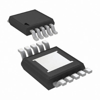
LM2833ZMY/NOPB National Semiconductor, LM2833ZMY/NOPB Datasheet - Page 15

LM2833ZMY/NOPB
Manufacturer Part Number
LM2833ZMY/NOPB
Description
IC REG BUCK 3.0MHZ 3A 10MSOP
Manufacturer
National Semiconductor
Type
Step-Down (Buck)r
Datasheet
1.LM2833XSDNOPB.pdf
(22 pages)
Specifications of LM2833ZMY/NOPB
Internal Switch(s)
Yes
Synchronous Rectifier
No
Number Of Outputs
1
Voltage - Output
0.6 ~ 4.5 V
Current - Output
3A
Frequency - Switching
3MHz
Voltage - Input
3 ~ 5.5 V
Operating Temperature
-40°C ~ 125°C
Mounting Type
Surface Mount
Package / Case
10-MSOP Exposed Pad, 10-HMSOP, 10-eMSOP
Lead Free Status / RoHS Status
Lead free / RoHS Compliant
Power - Output
-
Other names
LM2833ZMYTR
If the inductor ripple current is fairly small, the conduction
losses can be simplified to:
Switching losses are also associated with the internal power
switch. They occur during the switch on and off transition pe-
riods, where voltages and currents overlap resulting in power
loss. The simplest means to determine this loss is to empiri-
cally measuring the rise and fall times (10% to 90%) of the
switch at the switch node.
Switching Power Loss is calculated as follows:
The power loss required for operation of the internal circuitry
is given by:
I
3.2mA for the LM2833X, and 4.3mA for the LM2833Z.
An example of efficiency calculation for a typical application
is shown in Table 1:
Q
D is calculated to be 0.72
is the quiescent operating current, and is typically around
R
IND
T
T
V
I
DS(ON)
f
V
OUT
V
RISE
FALL
P
OUT
SW
I
η
Q
IN
D
DCR
LOSS
Conditions
P
P
TABLE 1. Power Loss Tabulation
SWR
= Σ ( P
SWF
P
= 0.5 x (V
= 0.5 x (V
COND
1.5MHz
COND
3.2mA
89.7%
56mΩ
28mΩ
0.33V
P
10ns
10ns
3.3V
3.0A
5V
SW
P
= I
LOSS
P
= P
+ P
Q
OUT
IN
IN
= I
SWR
SW
= 1.133W
x I
2
x I
Q
x R
OUT
OUT
x V
+ P
+ P
DS(ON)
P
P
IN
P
Q
x f
P
x f
P
DIODE
COND
P
SWF
OUT
SW
IND
+ P
Q
SW
SW
Power loss
IND
x D
x T
x T
+ P
RISE
FALL
DIODE
)
)
277mW
363mW
225mW
252mW
16mW
9.9W
)
15
PCB LAYOUT CONSIDERATIONS
When planning layout there are a few things to consider to
achieve a clean, regulated output. The most important con-
sideration is the close coupling of the GND connections of the
input capacitor C1 and the catch diode D1. These ground
ends should be close to one another and be connected to the
GND plane with at least two through-holes. Place these com-
ponents as close to the IC as possible. The next consideration
is the location of the GND connection of the output capacitor
C2, which should be near the GND connections of C1 and D1.
There should be a continuous ground plane on the bottom
layer of a two-layer board except under the switching node
island. The signal ground SGND (pin 3) and power ground
PGND (pin 6) should be tied together and connected to
ground plane through vias.
The FB pin is a high impedance node and care should be
taken to make the FB trace short to avoid noise pickup that
causes inaccurate regulation. The feedback resistors should
be placed as close as possible to the IC, with the GND of R2
placed as close as possible to the SGND of the IC. The
V
any other traces that are switching.
High AC currents flow through the V
so they should be as short and wide as possible. Radiated
noise can be decreased by choosing a shielded inductor.
The remaining components should also be placed as close
as possible to the IC. Please see Application Note AN-1229
for further considerations and the LM2833 demo board as an
example of a four-layer layout.
OUT
trace to R1 should be routed away from the inductor and
IN
, SW and V
www.national.com
OUT
traces,


