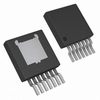
LM22670TJE-5.0/NOPB National Semiconductor, LM22670TJE-5.0/NOPB Datasheet - Page 13

LM22670TJE-5.0/NOPB
Manufacturer Part Number
LM22670TJE-5.0/NOPB
Description
IC REG SWITCH BUCK 3A 5V TO263-7
Manufacturer
National Semiconductor
Series
SIMPLE SWITCHER®r
Type
Step-Down (Buck)r
Datasheet
1.LM22670TJE-ADJNOPB.pdf
(20 pages)
Specifications of LM22670TJE-5.0/NOPB
Internal Switch(s)
Yes
Synchronous Rectifier
No
Number Of Outputs
1
Voltage - Output
5V
Current - Output
3A
Frequency - Switching
200kHz ~ 1MHz
Voltage - Input
4.5 ~ 42 V
Operating Temperature
-40°C ~ 125°C
Mounting Type
Surface Mount
Package / Case
TO-263-7 Thin
Primary Input Voltage
12V
No. Of Outputs
1
Output Voltage
5V
Output Current
3A
No. Of Pins
7
Operating Temperature Range
-40°C To +125°C
Msl
MSL 1 - Unlimited
Filter Terminals
SMD
Rohs Compliant
Yes
For Use With
551600233-001 - WEBENCH BUILD IT LM2267X TO-263LM22670INVEVAL - BOARD EVALUATION FOR LM22670INVLM22670EVAL - BOARD EVALUATION FOR LM22670
Lead Free Status / RoHS Status
Lead free / RoHS Compliant
Power - Output
-
Other names
LM22670TJE-5.0TR
Available stocks
Company
Part Number
Manufacturer
Quantity
Price
Company:
Part Number:
LM22670TJE-5.0/NOPB
Manufacturer:
AD
Quantity:
1 000
Part Number:
LM22670TJE-5.0/NOPB
Manufacturer:
TI/德州仪器
Quantity:
20 000
nected to the FB pin. Other output voltages can use the -ADJ
option with a resistor divider.
The resistor values can be determined by the following equa-
tions:
-ADJ option:
-5.0 option:
Where V
-5.0 option
A maximum value of 10 kΩ is recommended for the sum of
R1 and R2 to keep high output voltage accuracy for the –ADJ
option. A maximum of 2 kΩ is recommended for the -5.0 out-
put voltage option. For the 5V fixed output voltage option, the
total internal divider resistance is typically 9.93 kΩ.
At loads less than 5 mA, the boot capacitor will not hold
enough charge to power the internal high side driver. The
output voltage may droop until the boot capacitor is
recharged. Selecting a total feedback resistance to be below
3 kΩ will provide some minimal load and can keep the output
voltage from collapsing in such low load conditions.
Catch Diode
A Schottky type re-circulating diode is required for all
LM22670 applications. Ultra-fast diodes which are not Schot-
tky diodes are not recommended and may result in damage
to the IC due to reverse recovery current transients. The near
ideal reverse recovery characteristics and low forward volt-
age drop of Schottky diodes are particularly important diode
characteristics for high input voltage and low output voltage
applications common to the LM22670. The reverse recovery
characteristic determines how long the current surge lasts
each cycle when the N-channel MOSFET is turned on. The
reverse recovery characteristics of Schottky diodes mini-
mizes the peak instantaneous power in the switch occurring
during turn-on for each cycle. The resulting switching losses
are significantly reduced when using a Schottky diode. The
reverse breakdown rating should be selected for the maxi-
mum V
a diode with the reverse voltage rating of 1.3 times the max-
imum input voltage.
IN
FB
, plus some safety margin. A rule of thumb is to select
FIGURE 5. Resistive Feedback Divider
= 1.285V typical for the -ADJ option and 5V for the
30076023
13
The forward voltage drop has a significant impact on the con-
version efficiency, especially for applications with a low output
voltage. ‘Rated’ current for diodes varies widely from various
manufacturers. The worst case is to assume a short circuit
load condition. In this case the diode will carry the output cur-
rent almost continuously. For the LM22670 this current can
be as high as 4.2A (typical). Assuming a worst case 1V drop
across the diode, the maximum diode power dissipation can
be as high as 4.2W.
Circuit Board Layout
Board layout is critical for switching power supplies. First, the
ground plane area must be sufficient for thermal dissipation
purposes. Second, appropriate guidelines must be followed
to reduce the effects of switching noise. Switch mode con-
verters are very fast switching devices. In such devices, the
rapid increase of input current combined with the parasitic
trace inductance generates unwanted L di/dt noise spikes.
The magnitude of this noise tends to increase as the output
current increases. This parasitic spike noise may turn into
electromagnetic interference (EMI) and can also cause prob-
lems in device performance. Therefore, care must be taken
in layout to minimize the effect of this switching noise.
The most important layout rule is to keep the AC current loops
as small as possible.
converter. The top schematic shows a dotted line which rep-
resents the current flow during the FET switch on-state. The
middle schematic shows the current flow during the FET
switch off-state.
The bottom schematic shows the currents referred to as AC
currents. These AC currents are the most critical since current
is changing in very short time periods. The dotted lines of the
bottom schematic are the traces to keep as short as possible.
This will also yield a small loop area reducing the loop induc-
tance. To avoid functional problems due to layout, review the
PCB layout example. Providing 3A of output current in a very
low thermal resistance package such as the TO-263 THIN is
challenging considering the trace inductances involved. Best
results are achieved if the placement of the LM22670, the by-
pass capacitor, the Schottky diode and the inductor are
placed as shown in the example. It is also recommended to
use 2oz copper boards or thicker to help thermal dissipation
and to reduce the parasitic inductances of board traces.
It is very important to ensure that the exposed DAP on the
TO-263 THIN package is soldered to the ground area of the
PCB to reduce the AC trace length between the bypass ca-
pacitor ground and the ground connection to the LM22670.
Not soldering the DAP to the board may result in erroneous
operation due to excessive noise on the board.
Figure 6
shows the current flow of a buck
www.national.com


