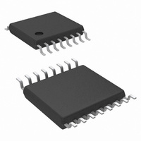
LM5088MH-2/NOPB National Semiconductor, LM5088MH-2/NOPB Datasheet - Page 16

LM5088MH-2/NOPB
Manufacturer Part Number
LM5088MH-2/NOPB
Description
IC BUCK ADJ 10A TSSOP16EP
Manufacturer
National Semiconductor
Series
PowerWise®r
Type
Step-Down (Buck)r
Datasheet
1.LM5088MH-1NOPB.pdf
(28 pages)
Specifications of LM5088MH-2/NOPB
Design Resources
LM(2)5088-1/2 QS Component Calculator
Internal Switch(s)
No
Synchronous Rectifier
No
Number Of Outputs
1
Voltage - Output
1.2 ~ 70 V
Current - Output
10A
Frequency - Switching
50kHz ~ 1MHz
Voltage - Input
4.5 ~ 75 V
Operating Temperature
-40°C ~ 125°C
Mounting Type
Surface Mount
Package / Case
16-TSSOP Exposed Pad, 16-eTSSOP, 16-HTSSOP
Lead Free Status / RoHS Status
Lead free / RoHS Compliant
Power - Output
-
Other names
LM5088MH-2
Available stocks
Company
Part Number
Manufacturer
Quantity
Price
Company:
Part Number:
LM5088MH-2/NOPB
Manufacturer:
TI
Quantity:
1 900
Part Number:
LM5088MH-2/NOPB
Manufacturer:
TI/德州仪器
Quantity:
20 000
www.national.com
Soft-Start
The soft-start (SS) feature forces the output to rise linearly
until it reaches the steady-state operating voltage set by the
feedback resistors. The LM5088 will regulate the FB pin to the
SS pin voltage or the internal 1.205V reference, which ever is
lower. At the beginning of the soft-start sequence VSS = 0V
and, an internal 11 µA current source gradually increases the
voltage of the external soft-start capacitor (C
amplifier clamps the SS pin voltage at 120 mV above the FB
voltage. This feature provides soft-start controlled recovery
with reduced output overshoot in the event that the output
voltage momentarily dips out of regulation.
HG Output
The LM5088 provides a high current, high-side driver and as-
sociated level shift circuit to drive an external N-Channel
MOSFET. The gate driver works in conjunction with an inter-
nal diode and external bootstrap capacitor. A ceramic boot-
strap capacitor is recommended, and should be connected
directly between the BOOT and SW pins. During the off-time
of the buck switch, the bootstrap capacitor charges from VCC
through an internal diode. When operating with a high PWM
duty cycle, the HG output will be forced-off each cycle for 365
ns (max) to ensure that BOOT capacitor is recharged. A “pre-
charge” circuit, comprised of a MOSFET between SW and
GND, is turned ON during the forced off-time to help replenish
the BOOT capacitor. The pre-charge circuit provides charge
to the BOOT capacitor under light load or pre-biased load
conditions when the SW voltage does not remain low during
the entire off-time.
Thermal Protection
Internal thermal shutdown circuitry is provided to protect the
integrated circuit in the event the maximum operating tem-
perature is exceeded. When activated, typically at 165°C, the
controller is forced into a low power reset state, disabling the
output driver and the bias supply of the controller. The feature
prevents catastrophic failures from accidental device over-
heating.
FIGURE 8. Current Limit Restart Timing Diagram
SS
). An internal
16
Applications Information
EXTERNAL COMPONENTS
The procedure for calculating the external components is il-
lustrated with the following design example. The Bill of Mate-
rials for this design is listed in Table 1.The circuit shown in
Figure 14 and 15 is configured for the following specifications:
•
•
•
•
TIMING RESISTOR
The RT resistor sets the oscillator switching frequency. High-
er frequencies result in smaller size components such as the
inductor and filter capacitors. However, operating at higher
frequencies also results in higher MOSFET and diode switch-
ing losses. Operation at 250 kHz was selected for this exam-
ple as a reasonable compromise between size and efficiency.
The value of RT resistor can be calculated as follows:
The nearest standard value of 24.9Ω was chosen for RT.
OUTPUT INDUCTOR
The inductor value is determined based on the operating fre-
quency, load current, ripple current and the input and output
voltages.
Knowing the switching frequency (f
rent (I
output voltage (V
follows:
Output Voltage = 5V
Input Voltage = 5.5V to 55V
Maximum Load Current = 7A
Switching Frequency = 250 kHz
PP
), maximum input voltage (VIN
OUT
), the inductor value can be calculated as
SW
), maximum ripple cur-
(max)
) and the nominal
30083917


