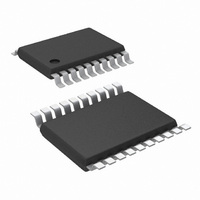
LM25116MH/NOPB National Semiconductor, LM25116MH/NOPB Datasheet - Page 17

LM25116MH/NOPB
Manufacturer Part Number
LM25116MH/NOPB
Description
IC CTRLR SYNC BUCK 20TSSOP
Manufacturer
National Semiconductor
Series
PowerWise®r
Type
Step-Down (Buck)r
Datasheet
1.LM25116MHNOPB.pdf
(26 pages)
Specifications of LM25116MH/NOPB
Internal Switch(s)
No
Synchronous Rectifier
Yes
Number Of Outputs
1
Voltage - Output
1.22 ~ 36 V
Current - Output
20A
Frequency - Switching
200kHz, 535kHz
Voltage - Input
6 ~ 42 V
Operating Temperature
-40°C ~ 125°C
Mounting Type
Surface Mount
Package / Case
20-TSSOP Exposed Pad, 20-eTSSOP, 20-HTSSOP
Primary Input Voltage
42V
No. Of Outputs
1
Output Voltage
36V
Output Current
20A
No. Of Pins
20
Operating Temperature Range
-40°C To +125°C
Msl
MSL 1 - Unlimited
Controller Type, Ic
Buck
Rohs Compliant
Yes
For Use With
LM25116EVAL - BOARD EVALUATION LM25116
Lead Free Status / RoHS Status
Lead free / RoHS Compliant
Power - Output
-
Other names
*LM25116MH
*LM25116MH/NOPB
LM25116MH
*LM25116MH/NOPB
LM25116MH
Available stocks
Company
Part Number
Manufacturer
Quantity
Price
Part Number:
LM25116MH/NOPB
Manufacturer:
NS/国半
Quantity:
20 000
ceptable. Higher ripple current allows for a smaller inductor
size, but places more of a burden on the output capacitor to
smooth the ripple current for low output ripple voltage. For this
example, 40% ripple current was chosen for a smaller sized
inductor.
The nearest standard value of 6µH will be used. The inductor
must be rated for the peak current to prevent saturation. Dur-
ing normal operation, the peak current occurs at maximum
load current plus maximum ripple. During overload conditions
with properly scaled component values, the peak current is
limited to V
input voltage with a shorted output, the valley current must fall
below V
to turn on. The peak current in steady state will increase to
V
must be evaluated for this condition, especially at elevated
temperature where the saturation current rating may drop sig-
nificantly.
CURRENT SENSE RESISTOR
The current limit is set by the current sense resistor value
(R
For a 5V output, the maximum current sense signal occurs at
the minimum input voltage, so R
For this example VCCX = 0V, so V
sense resistor is calculated as:
The next lowest standard value of 10mΩ was chosen for R
RAMP CAPACITOR
With the inductor and sense resistor value selected, the value
of the ramp capacitor (C
ramp circuit is:
Where L is the value of the output inductor in Henrys, g
the ramp generator transconductance (5µA/V), and A is the
current sense amplifier gain (10V/V). For the 5V output design
example, the ramp capacitor is calculated as:
IN(MAX)
S
).
CS(TH)
x t
ON(min)
CS(TH)
/ R
S
/ R
/ L above this level. The chosen inductor
before the high-side MOSFET is allowed
S
(See next section). At the maximum
RAMP
) necessary for the emulation
S
CS(TH)
is calculated from:
= 0.11V. The current
m
S
is
.
17
The next lowest standard value of 270pF was selected for
C
recommended.
OUTPUT CAPACITORS
The output capacitors smooth the inductor ripple current and
provide a source of charge for transient loading conditions.
For this design example, five 100µF ceramic capacitors
where selected. Ceramic capacitors provide very low equiv-
alent series resistance (ESR), but can exhibit a significant
reduction
manufacturer’s data, the ESR at 250kHz is 2mΩ / 5 =
0.4mΩ, with a 36% reduction in capacitance at 5V. This is
verified by measuring the output ripple voltage and frequency
response of the circuit. The fundamental component of the
output ripple voltage is calculated as:
With typical values for the 5V design example:
INPUT CAPACITORS
The regulator supply voltage has a large source impedance
at the switching frequency. Good quality input capacitors are
necessary to limit the ripple voltage at the VIN pin while sup-
plying most of the switch current during the on-time. When the
buck switch turns on, the current into the switch steps to the
valley of the inductor current waveform, ramps up to the peak
value, and then drops to zero at turn-off. The input capacitors
should be selected for RMS current rating and minimum ripple
voltage. A good approximation for the required ripple current
rating is I
Quality ceramic capacitors with a low ESR were selected for
the input filter. To allow for capacitor tolerances and voltage
rating, four 2.2µF ceramic capacitors were used for the typical
application circuit. With ceramic capacitors, the input ripple
voltage will be triangular and peak at 50% duty cycle. Taking
into account the capacitance change with DC bias, the input
ripple voltage is approximated as:
When the converter is connected to an input power source, a
resonant circuit is formed by the line impedance and the input
capacitors. If step input voltage transients are expected near
the maximum rating of the LM25116, a careful evaluation of
the ringing and possible overshoot at the device VIN pin
should be completed. To minimize overshoot make C
x L
quency are:
RAMP
IN
. The characteristic source impedance and resonant fre-
. A COG type capacitor with 5% or better tolerance is
RMS
in
> I
capacitance
OUT
/ 2.
with
DC
bias.
www.national.com
From
IN
> 10
the


