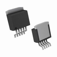
LM2587S-ADJ/NOPB National Semiconductor, LM2587S-ADJ/NOPB Datasheet - Page 18

LM2587S-ADJ/NOPB
Manufacturer Part Number
LM2587S-ADJ/NOPB
Description
IC REG SIMPLE SWITCHER TO-263-5
Manufacturer
National Semiconductor
Series
SIMPLE SWITCHER®r
Type
Step-Up (Boost), Flyback, Forward Converterr
Datasheet
1.LM2587S-ADJNOPB.pdf
(28 pages)
Specifications of LM2587S-ADJ/NOPB
Internal Switch(s)
Yes
Synchronous Rectifier
No
Number Of Outputs
1
Voltage - Output
Adjustable
Current - Output
5A
Frequency - Switching
100kHz
Voltage - Input
4 ~ 40 V
Operating Temperature
-40°C ~ 125°C
Mounting Type
Surface Mount
Package / Case
D²Pak, TO-263 (5 leads + tab)
Package
6TO-263
Minimum Input Voltage
4 V
Maximum Input Voltage
40 V
Switching Frequency
115 KHz
Operating Supply Voltage
4 to 40 V
Output Type
Adjustable
Output Voltage
1.23(Min) V
Efficiency
90(Typ) %
Primary Input Voltage
40V
No. Of Outputs
1
Output Current
5A
No. Of Pins
5
Operating Temperature Range
-40°C To +125°C
Msl
MSL 3 - 168 Hours
Filter Terminals
SMD
Rohs Compliant
Yes
For Use With
551011367-061 - BOARD WEBENCH LM2577,LM2585/87LM2587EVAL - EVALUATION BOARD FOR LM2587
Lead Free Status / RoHS Status
Lead free / RoHS Compliant
Power - Output
-
Other names
*LM2587S-ADJ
*LM2587S-ADJ/NOPB
LM2587S-ADJ
*LM2587S-ADJ/NOPB
LM2587S-ADJ
www.national.com
Step-Up (Boost) Regulator
Operation
Figure 33
ulator. This is a switching regulator that produces an output
voltage greater than the input supply voltage.
A brief explanation of how the LM2587 Boost Regulator works
is as follows (refer to
By adding a small number of external components (as shown in
the applied input voltage. The switching waveforms observed during the operation of this circuit are shown in
shown in
Figure
shows the LM2587 used as a step-up (boost) reg-
35.
Figure
33). When the NPN switch turns
FIGURE 33. 12V Boost Regulator
FIGURE 32. Schott 67140930
Figure
33), the LM2587 can be used to produce a regulated output voltage that is greater than
Top View
T4
18
on, the inductor current ramps up at the rate of V
energy in the inductor. When the switch turns off, the lower
end of the inductor flies above V
through diode (D) into the output capacitor (C
(V
switch on time is transferred to the output during the switch
off time. The output voltage is controlled by adjusting the peak
switch current, as described in the flyback regulator section.
OUT
− V
IN
)/L. Thus, energy stored in the inductor during the
1231647
Figure
34. Typical performance of this regulator is
IN
, discharging its current
1231619
OUT
) at a rate of
IN
/L, storing


