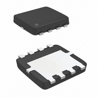
AOZ1014DI Alpha & Omega Semiconductor Inc, AOZ1014DI Datasheet - Page 13

AOZ1014DI
Manufacturer Part Number
AOZ1014DI
Description
IC 5A BUCK REG 8-DFN
Manufacturer
Alpha & Omega Semiconductor Inc
Series
EZBuck™r
Type
Step-Down (Buck)r
Datasheet
1.AOZ1014AI.pdf
(19 pages)
Specifications of AOZ1014DI
Internal Switch(s)
Yes
Synchronous Rectifier
No
Number Of Outputs
1
Voltage - Output
0.8 ~ 16 V
Current - Output
5A
Frequency - Switching
500kHz
Voltage - Input
4.5 ~ 16 V
Operating Temperature
-40°C ~ 85°C
Mounting Type
Surface Mount
Package / Case
8-DFN
Lead Free Status / RoHS Status
Lead free / RoHS Compliant
Power - Output
-
Other names
785-1150-2
Available stocks
Company
Part Number
Manufacturer
Quantity
Price
Part Number:
AOZ1014DI
Manufacturer:
AOS/万代
Quantity:
20 000
The actual junction temperature can be calculated
with power dissipation in the AOZ1014 and thermal
impedance from junction to ambient is:
The maximum junction temperature of AOZ1014 is
145°C, which limits the maximum load current capability.
Please see the thermal de-rating curves for maximum
load current of the AOZ1014 under different ambient
temperatures.
The thermal performance of the AOZ1014 is strongly
affected by the PCB layout. Extra care should be taken
by users during the design process to ensure that the IC
will operate under the recommended environmental
conditions.
Several layout tips are listed below for the best electric
and thermal performance. Figure 3 below illustrates a
PCB layout example as a reference.
1. Do not use thermal relief connection to the V
2. Input capacitor should be connected to the V
3. A ground plane is preferred. If a ground plane is not
4. Make the current trace from LX pins to L to Co to the
5. Pour copper plane on all unused board area and
6. The two LX pins are connected to the internal PFET
7. Keep sensitive signal traces away from the LX pins.
8. For the DFN package, thermal pad must be soldered
T
Rev. 1.2 October 2009
junction
the PGND pin. Pour a maximized copper area to
the PGND pin and the V
dissipation.
and the PGND pin as close as possible.
used, separate PGND from AGND and connect them
only at one point to avoid the PGND pin noise
coupling to the AGND pin.
PGND as short as possible.
connect it to stable DC nodes, like V
V
drain. They are low resistance thermal conduction
path and most noisy switching node. Connect a
copper plane to the LX pin to help thermal
dissipation. This copper plane should not be too
large otherwise switching noise may be coupled to
other parts of the circuit.
to the PCB metal. When multiple layer PCB is used,
4 to 6 thermal vias should be placed on the thermal
pad and connected to PCB metal on other layers to
help thermal dissipation.
OUT
.
=
(
P
total_loss
–
P
IN
inductor_loss
pin to help thermal
IN
, GND, or
) Θ
×
JA
IN
IN
www.aosmd.com
and
pin
Figure 4. AOZ1014 (DFN-8) PCB Layout
Figure 3. AOZ1014 (SO-8) PCB Layout
AOZ1014
Page 13 of 19


