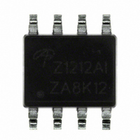
AOZ1212AI Alpha & Omega Semiconductor Inc, AOZ1212AI Datasheet - Page 7

AOZ1212AI
Manufacturer Part Number
AOZ1212AI
Description
IC 3A BUCK REG 8-SOIC
Manufacturer
Alpha & Omega Semiconductor Inc
Series
EZBuck™r
Type
Step-Down (Buck)r
Datasheet
1.AOZ1212DI.pdf
(18 pages)
Specifications of AOZ1212AI
Internal Switch(s)
Yes
Synchronous Rectifier
No
Number Of Outputs
1
Voltage - Output
0.8 ~ 27 V
Current - Output
3A
Frequency - Switching
370kHz
Voltage - Input
4.5 ~ 27 V
Operating Temperature
-40°C ~ 85°C
Mounting Type
Surface Mount
Package / Case
8-SOIC (3.9mm Width)
Lead Free Status / RoHS Status
Lead free / RoHS Compliant
Power - Output
-
Other names
785-1159-2
Available stocks
Company
Part Number
Manufacturer
Quantity
Price
Company:
Part Number:
AOZ1212AI
Manufacturer:
AO
Quantity:
1 000
Part Number:
AOZ1212AI
Manufacturer:
AOS/万代
Quantity:
20 000
Company:
Part Number:
AOZ1212AIL
Manufacturer:
ALPHA&OMEGA
Quantity:
257
Detailed Description
The AOZ1212 is a current-mode step down regulator
with integrated high side NMOS switch. It operates from
a 4.5V to 27V input voltage range and supplies up to 3A
of load current. The duty cycle can be adjusted from 6%
to 85% allowing a wide range of output voltages. Fea-
tures include enable control, Power-On Reset, input
under voltage lockout, fixed internal soft-start and ther-
mal shut down.
The AOZ1212 is available in an SO-8 or DFN-8 package.
Enable and Soft Start
The AOZ1212 has an internal soft start feature to limit
in-rush current and ensure the output voltage ramps up
smoothly to the regulation voltage. A soft start process
begins when the input voltage rises to 4.1V and voltage
on EN pin is HIGH. In the soft start process, the output
voltage is typically ramped to regulation voltage in 6.8ms.
The 6.8ms soft start time is set internally.
If the enable function is not used, connect the EN pin to
V
not leave EN open. The voltage on the EN pin must be
above 2.5 V to enable the AOZ1212. When voltage on
EN pin falls below 0.6V, the AOZ1212 is disabled. If an
application circuit requires the AOZ1212 to be disabled,
an open drain or open collector circuit should be used to
interface with the EN pin.
Steady-State Operation
Under steady-state conditions, the converter operates in
fixed frequency and Continuous-Conduction Mode
(CCM).
The AOZ1212 integrates an internal N-MOSFET as the
high-side switch. Inductor current is sensed by amplifying
the voltage drop across the drain to source of the high
side power MOSFET. Since the N-MOSFET requires a
gate voltage higher than the input voltage, a boost
capacitor connected between the LX and BST pins drives
the gate. The boost capacitor is charged while LX is low.
An internal 10
that LX is pulled to GND even in the light load. Output
voltage is divided down by the external voltage divider at
the FB pin. The difference of the FB pin voltage and
reference is amplified by the internal transconductance
error amplifier. The error voltage, which shows on the
COMP pin, is compared against the current signal. The
current signal is the sum of inductor current signal and
ramp compensation signal, at the PWM comparator
input. If the current signal is less than the error voltage,
the internal high-side switch is on. The inductor current
flows from the input through the inductor to the output.
When the current signal exceeds the error voltage, the
IN
Rev. 1.7 November 2010
. Pulling EN to ground will disable the AOZ1212. Do
Ω
switch from LX to GND is used to ensure
www.aosmd.com
high-side switch is off. The inductor current is free-
wheeling through the Schottky diode to the output.
Switching Frequency
The AOZ1212 switching frequency is fixed and set by
an internal oscillator. The switching frequency is set to
370kHz.
Output Voltage Programming
Output voltage can be set by feeding back the output to
the FB pin with a resistor divider network. In the applica-
tion circuit shown in Figure 1. The resistor divider
network includes R
by picking a fixed R
R
Some standard values for R
commonly used output voltages are listed in Table 1.
Table 1.
The combination of R
avoid drawing excessive current from the output, which
will cause power loss.
Protection Features
The AOZ1212 has multiple protection features to prevent
system circuit damage under abnormal conditions.
Over Current Protection (OCP)
The sensed inductor current signal is also used for over
current protection. Since the AOZ1212 employs peak
current mode control, the COMP pin voltage is propor-
tional to the peak inductor current. The COMP pin volt-
age is limited to be between 0.4V and 2.5V internally.
The peak inductor current is automatically limited cycle
by cycle.
The cycle-by-cycle current limit threshold is internally set.
When the load current reaches the current limit thresh-
old, the cycle-by-cycle current limit circuit turns off the
V
0.8
1.2
1.5
1.8
2.5
3.3
5.0
1
O
value with equation below.
=
V
0.8
O
(V)
×
⎛
⎜
⎝
1
+
1
R
------ -
R
2
1.0
4.99
10
12.7
21.5
31.6
52.3
and R
1
2
value and calculating the required
1
⎞
⎟
⎠
and R
R
1
2
. Typically, a design is started
(k
1
2
and R
Ω
should be large enough to
)
2
for the most
Open
10
11.5
10.2
10
10
10
AOZ1212
R
Page 7 of 18
2
(k
Ω
)


