IR3870MTR1PBF International Rectifier, IR3870MTR1PBF Datasheet
IR3870MTR1PBF
Specifications of IR3870MTR1PBF


Related parts for IR3870MTR1PBF

IR3870MTR1PBF Summary of contents
Page 1
SupIRBuck TM WIDE-INPUT VOLTAGE, SYNCHRONOUS BUCK REGULATOR Features • Input Voltage Range 26V • Output Voltage Range: 0.5V to 12V • Continuous 10A Load Capability • Constant On-Time control • Excellent Efficiency at very low output current levels ...
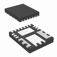
Page 2
... These are stress ratings only and functional operation of the device at these or any other conditions beyond those indicated in the operational sections of the specifications are not implied. PACKAGE INFORMATION 5mm x 6mm POWER QFN ORDERING INFORMATION PKG DESIG DESCRIPTION M IR3870MTRPbF M IR3870MTR1PbF PACKAGE PIN COUNT 23 23 IR3870MBF θ ...
Page 3
Block Diagram IR3870MBF 3 ...
Page 4
Pin Description NAME NUMBER I/O LEVEL NC 1 ISET 2 PGOOD 3 5V GND 4,17 Reference VCC 8 3.3V CPO 9 0.75V PVCC 10 5V PGND 11 Reference PHASE 12 VIN VIN ...
Page 5
Recommended Operating Conditions Symbol Definition VIN Input Voltage VCC Supply Voltage Boot to Supply Voltage PHASE V Output Voltage OUT I Output Current OUT Fs Switching Frequency * Note: PHASE pin must not exceed 30V. Electrical Specifications Unless otherwise specified, ...
Page 6
Electrical Specifications (continued) Unless otherwise specified, these specification apply over VIN = 12V, PVCC = 7VDC, 0 PARAMETER NOTE GATE DRIVE Dead time UPPER MOSFET Static Drain-to-Source On- Resistance Static Drain-to-Source On- Resistance Static Drain-to-Source On- Resistance Static Drain-to-Source On- ...
Page 7
TYPICAL OPERATING DATA (25 (Circuit of Figure 15, VCC = 3.3V 5V, V 1000000 1000000 1000 1000 , , Rff 0.5 fsw Rff 0.5 fsw ( ( ) ) , , Rff 1 fsw Rff 1 fsw ( ...
Page 8
TYPICAL OPERATING DATA (25 (Circuit of Figure 15, VCC = 3.3V 5V, V 1.11400 1.10900 1.10400 1.09900 1.09400 1.08900 Output Current (A) Figure 5. Output Voltage Regulation Vs Output Current Eff: 12.6Vin Eff: 19Vin ...
Page 9
TYPICAL OPERATING WAVEFORM (25 (Circuit of Figure 15, VCC = 3.3V 5V, V CH1: Vout (500mV/div); 500uS/div CH2: PHASE (10V/div) CH3: EN (2V/div) CH4: PGOOD (5V/div) Figure 9: Shutdown/ 500mA OUT CH1: Vout (50mV/div); 20uS/div ...
Page 10
TYPICAL OPERATING WAVEFORM con’t (25 (Circuit of Figure 15, VCC = 3.3V 5V, V CH1: Vout (50mV/div); CH2: Phase (10V/div) CH4: CPO (2V/div); Time: 2uS/div) Figure 13: Charge Pump IC Inductor: 53 ...
Page 11
TYPICAL APPLICATION CIRCUIT WITH CHARGE PUMP OPTION Figure 15. Application Circuit with Charge Pump used to boost Sync FET gate drive voltage from 5V to ~7V, resulting in improved efficiency at higher output current levels F = 500kHz ...
Page 12
Circuit Description PWM COMPARATOR The PWM comparator initiates a SET signal (PWM pulse) when the FB pin falls below the reference (VREF) or the soft start (SS) voltage. ON-TIME GENERATOR The PWM comparator initiates a SET signal (PWM pulse) when ...
Page 13
Circuit Description voltage is within regulation before four consecutive soft-start cycles, PGOOD transitions HIGH to reset the counter. OVER VOLTAGE PROTECTION The IR3870 monitors the voltage at the FB node. If the FB voltage is above the over voltage threshold, ...
Page 14
Output Capacitor Selection Selection of the output capacitor requires meeting voltage overshoot requirements during load removal, and meeting steady state output ripple voltage requirements. The output capacitor is the most expensive converter component and increases the overall system cost. The ...
Page 15
Boot Capacitor Selection The boot capacitor starts the cycle fully charged to a voltage of VB(0). Cg equals 1.16nF in IR3870. Choose a sufficiently small ΔV such that VB(0)-ΔV exceeds the maximum gate threshold voltage to turn on the high ...
Page 16
This capacitor has 9mΩ ESR which leaves margin for the voltage drop of the ESL during load step up. The typical ESL for this capacitor is around 2nH. Refer to Output Capacitor Selection section for all ceramic capacitor solution. LAYOUT ...
Page 17
PCB Metal and Components Placement Lead lands (the 13 IC pins) width should be equal to nominal part lead width. The minimum lead to lead spacing should be ≥ 0.2mm to minimize shorting. Lead land length should be equal to ...
Page 18
Solder Resist It is recommended that the lead lands are Non Solder Mask Defined (NSMD). The solder resist should be pulled away from the metal lead lands by a minimum of 0.025mm to ensure NSMD pads. The land pad should ...
Page 19
Stencil Design The Stencil apertures for the lead lands should be approximately 80% of the area of the lead lads. Reducing the amount of solder deposited will minimize the occurrences of lead shorts. If too much solder is deposited on ...
Page 20
MILIMITERS DIM MIN MAX MIN A 0.8 1 0.0315 0.375 0.475 0.1477 b1 0.25 0.35 0.0098 c 0.203 REF. D 5.000 BASIC 1.970 BASIC E 6.000 BASIC 2.364 BASIC e 1.033 BASIC 0.0407 BASIC e1 ...