IR3870MTR1PBF International Rectifier, IR3870MTR1PBF Datasheet - Page 12
IR3870MTR1PBF
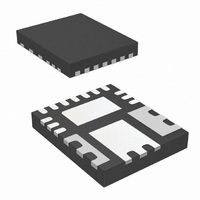
Manufacturer Part Number
IR3870MTR1PBF
Description
IC BUCK SYNC ADJ 10A PQFN56
Manufacturer
International Rectifier
Series
SupIRBuck™r
Type
Step-Down (Buck)r
Datasheet
1.IR3870MTR1PBF.pdf
(20 pages)
Specifications of IR3870MTR1PBF
Internal Switch(s)
Yes
Synchronous Rectifier
Yes
Number Of Outputs
1
Voltage - Output
0.5 ~ 12 V
Current - Output
10A
Frequency - Switching
200kHz ~ 1MHz
Voltage - Input
3 ~ 26 V
Operating Temperature
0°C ~ 125°C
Mounting Type
Surface Mount
Package / Case
17-PowerVQFN
Part Status
Active
Package
PQFN / 5 x 6
Circuit
Single Output
Iout (a)
10
Switch Freq (khz)
0 - 1000
Input Range (v)
3.0 - 26
Output Range (v)
0.5 - 12
Ocp Otp Uvlo Pre-bias Soft Start And
Constant On-Time + OVP no OTP
Lead Free Status / RoHS Status
Lead free / RoHS Compliant
Power - Output
-
Other names
IR3870MTR1PBFTR


Circuit Description
PWM COMPARATOR
The PWM comparator initiates a SET signal
(PWM pulse) when the FB pin falls below the
reference (VREF) or the soft start (SS) voltage.
ON-TIME GENERATOR
The PWM comparator initiates a SET signal
(PWM pulse) when the FB pin falls below the
reference (VREF) or the soft start (SS) voltage.
The PWM on-time duration is programmed with
an external resistor (RFF) from the input supply
(VIN) to the FF pin. The simplified equation for
RFF is shown in equation 1. The FF pin is held
to an internal reference after EN goes HIGH. A
copy of the current in RFF charges a timing
capacitor, which sets the on-time duration, as
shown in equation 2.
SOFT START
An internal 10uA current source charges the
external capacitor on the SS pin to set the output
voltage slew rate during the soft start interval.
The output voltage reaches regulation when the
FB pin is above the under voltage threshold and
the UV# = HIGH. Once the voltage on the SS pin
is above the PGOOD delay threshold, the
combination of the SSDelay and UV# signals
release the PGOOD pin. With EN = LOW, the
capacitor voltage and SS pin is held to the FB pin
voltage.
OVER CURRENT MONITOR
The over current circuitry monitors the output
current during each switching cycle. The voltage
across the synchronous MOSFET, VPHASE, is
monitored for over current and zero crossing.
The minimum LGATE interval allows time to
sample VPHASE.
The over current trip point is programmed with a
resistor from the ISET pin to PHASE pin, as
shown in equation 3. When over current is
detected, the output gates are tri-state and SS
voltage is pulled to 0V. This initiates a new soft
start cycle. If there are three consecutive OC
events the IR3870 will disable switching.
Toggling VCC or EN will allow the next start up.
R
T
ON
FF
=
=
1
R
V
FF
⋅
20
⋅
V
1
V
V ⋅
OUT
pF
IN
20
⋅
F
SW
pF
(2)
(1)
GATE DRIVE LOGIC
The gate drive logic features adaptive dead time,
diode emulation, and a minimum lower gate
interval.
An adaptive dead time prevents the simultaneous
conduction of the upper and lower MOSFETs.
The lower gate voltage must be below
approximately 1V after PWM goes HIGH before
the upper MOSFET can be gated on. Also, the
upper gate voltage, the difference voltage
between UGATE and PHASE, must be below
approximately 1V after PWM goes LOW and
before the lower MOSFET can be gated on.
The control MOSFET is gated on after the
adaptive delay for PWM = HIGH and the
synchronous MOSFET is gated on after the
adaptive delay for PWM = LOW. The lower
MOSFET is driven ‘off’ when the signal ZCROSS
indicates that the inductor current has reversed
as detected by the PHASE voltage crossing the
zero current threshold. The synchronous
MOSFET stays ‘off’ until the next PWM falling
edge. When the lower peak of inductor current is
above zero, a forced continuous current condition
is selected set. The control MOSFET is gated on
after the adaptive delay for PWM = HIGH, and
the synchronous MOSFET is gated on after the
adaptive delay for PWM = LOW.
The synchronous MOSFET gate is driven on for
a minimum duration. This minimum duration
allows time to recharge the bootstrap capacitor
and allows the current monitor to sample the
phase voltage.
CONTROL LOGIC
The control logic monitors input power sources,
sequences the converter through the soft-start
and protective modes and indicates output
voltage status on the PGOOD pin. PVCC and
VCC pins are continuously monitored and will
disable the IR3870 if the voltage of either pin
drops below the falling thresholds.
The IR3870 will initiate a soft start when the
PVCC is in the normal range and the EN pin =
HIGH. In the event of a sustained overload a
counter keeps track of 4 consecutive soft-start
cycles and then disables the IR3870.
If the overload is momentary and the output
R
SET
=
R
DSON
20
⋅
μ
I
A
OC
(3)
IR3870MBF
12
Related parts for IR3870MTR1PBF
Image
Part Number
Description
Manufacturer
Datasheet
Request
R

Part Number:
Description:
SCHOTTKY RECTIFIER
Manufacturer:
International Rectifier Corp.
Datasheet:
Part Number:
Description:
SCHOTTKY RECTIFIER
Manufacturer:
International Rectifier Corp.
Datasheet:
Part Number:
Description:
SCHOTTKY RECTIFIER
Manufacturer:
International Rectifier Corp.
Datasheet:
Part Number:
Description:
SCHOTTKY RECTIFIER
Manufacturer:
International Rectifier Corp.
Datasheet:
Part Number:
Description:
SCHOTTKY RECTIFIER
Manufacturer:
International Rectifier Corp.
Datasheet:
Part Number:
Description:
SCHOTTKY RECTIFIER
Manufacturer:
International Rectifier Corp.
Datasheet:
Part Number:
Description:
SCHOTTKY RECTIFIER
Manufacturer:
International Rectifier Corp.
Datasheet:
Part Number:
Description:
SCHOTTKY RECTIFIER
Manufacturer:
International Rectifier Corp.
Datasheet:
Part Number:
Description:
SCHOTTKY RECTIFIER
Manufacturer:
International Rectifier Corp.
Datasheet:
Part Number:
Description:
SCHOTTKY RECTIFIER
Manufacturer:
International Rectifier Corp.
Datasheet:
Part Number:
Description:
SCHOTTKY RECTIFIER
Manufacturer:
International Rectifier Corp.
Datasheet:
Part Number:
Description:
SCHOTTKY RECTIFIER
Manufacturer:
International Rectifier Corp.
Datasheet:
Part Number:
Description:
SCHOTTKY RECTIFIER
Manufacturer:
International Rectifier Corp.
Datasheet:
Part Number:
Description:
SCHOTTKY RECTIFIER
Manufacturer:
International Rectifier Corp.
Datasheet:
Part Number:
Description:
SCHOTTKY RECTIFIER
Manufacturer:
International Rectifier Corp.
Datasheet: