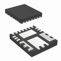
IR3870MTR1PBF International Rectifier, IR3870MTR1PBF Datasheet - Page 13

IR3870MTR1PBF
Manufacturer Part Number
IR3870MTR1PBF
Description
IC BUCK SYNC ADJ 10A PQFN56
Manufacturer
International Rectifier
Series
SupIRBuck™r
Type
Step-Down (Buck)r
Datasheet
1.IR3870MTR1PBF.pdf
(20 pages)
Specifications of IR3870MTR1PBF
Internal Switch(s)
Yes
Synchronous Rectifier
Yes
Number Of Outputs
1
Voltage - Output
0.5 ~ 12 V
Current - Output
10A
Frequency - Switching
200kHz ~ 1MHz
Voltage - Input
3 ~ 26 V
Operating Temperature
0°C ~ 125°C
Mounting Type
Surface Mount
Package / Case
17-PowerVQFN
Part Status
Active
Package
PQFN / 5 x 6
Circuit
Single Output
Iout (a)
10
Switch Freq (khz)
0 - 1000
Input Range (v)
3.0 - 26
Output Range (v)
0.5 - 12
Ocp Otp Uvlo Pre-bias Soft Start And
Constant On-Time + OVP no OTP
Lead Free Status / RoHS Status
Lead free / RoHS Compliant
Power - Output
-
Other names
IR3870MTR1PBFTR
Circuit Description
COMPONENT SELECTION
Selection of components for the converter is an
iterative process which involves meeting the
specifications and trade-offs between performance
and cost. The following sections will guide one
through the process.
Inductor Selection
Inductor selection involves meeting the steady
state output ripple requirement, minimizing the
switching loss of upper MOSFETs, meeting
transient response specifications and minimizing
the output capacitance. The output voltage
includes a DC voltage and a small AC ripple
component due to the low pass filter which has
incomplete attenuation of the switching harmonics.
Neglecting the inductance in series with the output
capacitor, the magnitude of the AC voltage ripple is
determined by the total inductor ripple current flow
through the total equivalent series resistance
(ESR) of the output capacitor bank.
voltage is within regulation before four
consecutive soft-start cycles, PGOOD transitions
HIGH to reset the counter.
OVER VOLTAGE PROTECTION
The IR3870 monitors the voltage at the FB node.
If the FB voltage is above the over voltage
threshold, the gates are turned off and the
PGOOD signal is pulled low. Toggling VCC will
allow the next start up.
CHARGE PUMP
The purpose of the charge pump is to improve
the system efficiency. A combination of VCC, V5
and three external components are used to boost
PVCC up to V
synchronous MOSFET and reduces the R
when compared to a regular 5V rail driver. The
lower FET RDSON reduces the conduction
power loss as discussed in the Power Loss
section. The charge pump is continuously
enabled for FCCM = HIGH. The charge pump
circuit is disabled when FCCM = LOW and the
output loading is less than half of inductor current
ripple. In this case, PVCC is two diode voltages
away from the V5 rail. Therefore, the power loss
for driver is reduced. The charge pump circuit
stops switching the CPO pin for PVCC above
V
ΔI
CPTH
=
V
.
OUT
L
⋅
(
1
−
CPTH
D
)
⋅
. PVCC drives the
Ts
=
V
OUT
V
⋅
IN
(
V
⋅
IN
L
⋅
−
F
V
s
OUT
DSON
)
(4)
One can use equation 4 to find the required
inductance. The main advantage of small
inductance is increased inductor current slew
rate during a load transient, which leads to a
smaller output capacitance requirement as
discussed in the Output Capacitor Selection
section. The draw back of using smaller
inductances is increased switching power loss in
upper MOSFET, which reduces the system
efficiency and increases the thermal dissipation
as discussed in the Power Loss section.
Input Capacitor Selection
The main function of the input capacitor bank is
to provide the input ripple current and fast slew
rate current during the load current step up. The
input capacitor bank must have adequate ripple
current carrying capability to handle the total
RMS current. Figure 16 shows a typical input
current. Equation 5 shows the RMS input current.
The RMS input current contains the DC load
current and the inductor ripple current. As shown
in equation 4, the inductor ripple current is
unrelated to the load current. The maximum
RMS input current occurs at the maximum output
current. The maximum power dissipation in the
input capacitor equals the square of the
maximum RMS input current times the input
capacitor’s total ESR.
Figure 16. Typical Input Current Waveform.
The voltage rating of the input capacitor needs to be
greater than the maximum input voltage because of
high frequency ringing at the phase node. The typical
percentage is 25%.
I
=
IN_RMS
I
OUT
⋅
=
D
⋅
Ts
1
1
+
⋅
Ts
∫
0
3
1
f
⋅
2
⎛
⎜
⎝
( )
I
t
IR3870MBF
OUT
ΔI
⋅
dt
⎞
⎟
⎠
2
(5)
13


