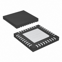
MAX8654ETX+ Maxim Integrated Products, MAX8654ETX+ Datasheet - Page 14

MAX8654ETX+
Manufacturer Part Number
MAX8654ETX+
Description
IC REG STP DWN 12V 8A 36TQFN
Manufacturer
Maxim Integrated Products
Type
Step-Down (Buck)r
Datasheet
1.MAX8654ETX.pdf
(17 pages)
Specifications of MAX8654ETX+
Internal Switch(s)
Yes
Synchronous Rectifier
No
Number Of Outputs
1
Voltage - Output
0.6 ~ 11.9 V
Current - Output
8A
Frequency - Switching
250kHz ~ 1.2MHz
Voltage - Input
4.5 ~ 14 V
Operating Temperature
-40°C ~ 85°C
Mounting Type
Surface Mount
Package / Case
36-TQFN Exposed Pad
Power - Output
2.86W
Output Voltage
0.6 V to 0.85 V
Output Current
8 A
Input Voltage
4.5 V to 14 V
Switching Frequency
1 MHz
Operating Temperature Range
- 40 C to + 85 C
Mounting Style
SMD/SMT
Lead Free Status / RoHS Status
Lead free / RoHS Compliant
12V, 8A 1.2MHz
Step-Down Regulator
output voltage divided by the rated output current. ESR
is the total equivalent series resistance (ESR) of the out-
put filtering capacitor. If there is more than one output
capacitor of the same type in parallel, the value of the
ESR in the above equation is equal to that of the ESR of
a single output capacitor divided by the total number of
output capacitors.
The high-switching frequency range of the MAX8654
allows the use of ceramic-output capacitors. Since the
ESR of ceramic capacitors is typically very low, the fre-
quency of the associated transfer function zero is higher
than the unity-gain crossover frequency, f
zero cannot be used to compensate for the double pole
created by the output filtering inductor and capacitor.
The double pole produces a gain drop of 40dB and a
phase shift of 180° per decade. The error amplifier must
compensate for this gain drop and phase shift to
achieve a stable high-bandwidth, closed-loop system.
Therefore, use type 3 compensation as shown in Figure
3. Type 3 compensation possesses three poles and two
zeros with the first pole, f
cy (DC). Locations of other poles and zeros of the type
3 compensation are given by:
The above equations are based on the assumptions
that C1>>C2 and R3>>R2 are true in most applica-
tions. Placements of these poles and zeros are deter-
mined by the frequencies of the double pole and ESR
zero of the power-transfer function. It is also a function
of the desired closed-loop bandwidth. The following
section outlines the step-by-step design procedure to
calculate the required compensation components for
the MAX8654.
Begin by setting the desired output voltage. The output
voltage is set using a resistor-divider from the output to
GND with FB at the center tap (R3 and R4 in Figure 3).
Calculate R4 as:
14
______________________________________________________________________________________
f
f
f
f
P
P
Z EA
Z
1
2
3
2
R
_
_
_
_
4
EA
EA
EA
=
=
=
=
V
=
P1_EA
0 6
OUT
2
2
2
2
.
π
π
π
π
x R x C
×
x R x C
x R x C
x R x C
−
, located at zero frequen-
R
1
1
0 6
1
1
1
1
2
3
3
.
1
2
3
3
C
, and the
The zero-cross frequency of the closed loop, f
be less than 20% of the switching frequency, f
zero-cross frequency results in faster transient
response. It is recommended that the zero-cross fre-
quency of the closed loop should be chosen between
10% and 20% of the switching frequency. Once f
chosen, C1 is calculated from the following equation:
Due to the underdamped nature of the output LC dou-
ble pole, set the two zero frequencies of the type 3
compensation less than the LC double-pole frequency
in order to provide adequate phase boost. Set the two
zero frequencies to 80% of the LC double-pole frequen-
cy. Hence:
Set the second compensation pole, f
yields:
Set the third compensation pole at the switching fre-
quency. Calculate C2 as follows:
Figure 3. Type 3 Compensation Network
R
C
MAX8654
1
3
=
=
0 8
0 8
.
C
.
1
COMP
1
x C
1
=
x R
LX
FB
2
1
R
C
3
x
2
2
x
x
=
π
=
L x C
x R x
C
1 5625
π
L x C
.
O
×
R1
3
C
x ESR
R
L
O
3
1
C2
R
O
C
R
1
L
OUT
(
x R
×
x V
1
L
x R
(
+
+
f
C1
S
(
+
IN
R
R
R
O
×
R
O
O
O
L
+
O
2
)
+
ESR
×
P2_EA
ESR
R3
f
C
)
)
, at f
R4
C
S
. Higher
, should
Z_ESR
V
OUT
R2
C
C3
is


