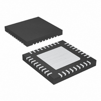
MAX8654ETX+ Maxim Integrated Products, MAX8654ETX+ Datasheet - Page 8

MAX8654ETX+
Manufacturer Part Number
MAX8654ETX+
Description
IC REG STP DWN 12V 8A 36TQFN
Manufacturer
Maxim Integrated Products
Type
Step-Down (Buck)r
Datasheet
1.MAX8654ETX.pdf
(17 pages)
Specifications of MAX8654ETX+
Internal Switch(s)
Yes
Synchronous Rectifier
No
Number Of Outputs
1
Voltage - Output
0.6 ~ 11.9 V
Current - Output
8A
Frequency - Switching
250kHz ~ 1.2MHz
Voltage - Input
4.5 ~ 14 V
Operating Temperature
-40°C ~ 85°C
Mounting Type
Surface Mount
Package / Case
36-TQFN Exposed Pad
Power - Output
2.86W
Output Voltage
0.6 V to 0.85 V
Output Current
8 A
Input Voltage
4.5 V to 14 V
Switching Frequency
1 MHz
Operating Temperature Range
- 40 C to + 85 C
Mounting Style
SMD/SMT
Lead Free Status / RoHS Status
Lead free / RoHS Compliant
12V, 8A 1.2MHz
Step-Down Regulator
8
1, 2, 3, 34,
35, 36
13, 32
30, 33
22–29
_______________________________________________________________________________________
PIN
5–8
10
11
12
14
15
16
17
18
19
20
21
31
—
4
9
SYNCOUT
PWRGD
NAME
COMP
PGND
REFIN
SYNC
FREQ
GND
ILIM
N.C.
VDL
BST
EN
VP
SS
FB
EP
VL
LX
IN
Power Ground. All PGND pins are internally connected. Connect all PGND pins externally to the power
ground plane.
5V LDO Output. VDL supplies the gate-drive current to the internal MOSFETS, and charges the BST
capacitor. VDL requires at least a 2.2μF ceramic bypass capacitor to PGND.
Power-Supply Input. Input supply range is from 4.5V to 14V. Bypass with two 10μF and a 0.1μF ceramic
capacitors to PGND. See Figure 1.
Input of the Internal 5V LDO Regulator. Connect to IN if a 5V supply is not available. Connect to an external
5V supply to disable the internal 5V regulator.
3.3V LDO for Internal Chip Supply. Bypass with a 1μF ceramic capacitor to GND.
Current-Limit Adjust. Connect a resistor, R
LX current-limit trip point. See the Current Limit section for more details.
Oscillator Frequency Selection. Connect a resistor from FREQ to GND to set the internal oscillator
frequency. See the Frequency Select (FREQ) section for more details.
Analog Circuit Ground
External Reference Input. Connect to an external reference. FB regulates to the voltage applied to REFIN.
Connect REFIN to SS to use the internal 0.6V reference. REFIN is internally pulled to GND when the IC is in
shutdown mode.
Soft-Start Input. Connect a capacitor from SS to GND to set the startup time. See the Soft-Start and REFIN
section for details.
Regulator Compensation. Connect the necessary compensation network from COMP to FB. COMP is
internally pulled to GND when the IC is in shutdown mode.
Feedback Input. Connect to the center tap of an external resistor-divider from the output to GND to set the
output voltage. See the Compensation Design section for more details.
Power-Good Output. Open-drain output that is high impedance when V
540mV. PWRGD is internally pulled low when the IC is in shutdown mode, or when V
below the UVLO threshold, or the IC is in thermal shutdown.
Oscillator Output. The SYNCOUT output is 180° out-of-phase from the internal oscillator to facilitate running
a second regulator out-of-phase to reduce input ripple.
Synchronization Input. Synchronize to an external clock with a frequency of 250kHz to 1.2MHz. Connect
SYNC to GND to disable the synchronization function.
High-Side MOSFET Driver Supply. Bypass BST to LX with a 0.22μF ceramic capacitor.
Inductor Connection. All LX pins are internally connected together. Connect all LX pins to the switched
side of the inductor. LX is high impedance when the IC is in shutdown mode.
Not Internally Connected
Enable Input. Logic input to enable/disable the MAX8654. Drive EN high to enable the IC. Drive EN low to
place the IC in a low-power shutdown mode.
Exposed Pad. Connect to a large PGND ground plane to optimize thermal performance. EP is internally
connected to GND and PGND.
ILIM
, from ILIM to GND. I
FUNCTION
ILIM
= 1V / R
FB
≥ 90% of V
ILIM
Pin Description
. I
VDL
ILIM
REFIN
, V
determines the
IN
and V
, or V
REFIN
VL
is
>


