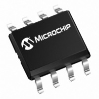
MCP1612-ADJI/MS Microchip Technology, MCP1612-ADJI/MS Datasheet - Page 10

MCP1612-ADJI/MS
Manufacturer Part Number
MCP1612-ADJI/MS
Description
IC BUCK REG ADJ 1A 1.4MHZ 8MSOP
Manufacturer
Microchip Technology
Type
Step-Down (Buck)r
Datasheet
1.MCP1612-ADJIMS.pdf
(22 pages)
Specifications of MCP1612-ADJI/MS
Package / Case
8-MSOP, Micro8™, 8-uMAX, 8-uSOP,
Internal Switch(s)
Yes
Synchronous Rectifier
Yes
Number Of Outputs
1
Voltage - Output
0.8 ~ 5 V
Current - Output
1A
Frequency - Switching
1.4MHz
Voltage - Input
2.7 ~ 5.5 V
Operating Temperature
-40°C ~ 85°C
Mounting Type
Surface Mount
Output Voltage
0.8 V to 5.5 V
Output Current
1 A
Input Voltage
2.7 V to 5.5 V
Switching Frequency
1.4 MHz
Operating Temperature Range
- 40 C to + 85 C
Mounting Style
SMD/SMT
Duty Cycle (max)
100 %
Lead Free Status / RoHS Status
Lead free / RoHS Compliant
Power - Output
-
Lead Free Status / Rohs Status
Lead free / RoHS Compliant
Available stocks
Company
Part Number
Manufacturer
Quantity
Price
Company:
Part Number:
MCP1612-ADJI/MS
Manufacturer:
MICROCHIP
Quantity:
12 000
Part Number:
MCP1612-ADJI/MS
Manufacturer:
MICROCHIP/微芯
Quantity:
20 000
MCP1612
4.0
4.1
The MCP1612 is a 1A synchronous buck converter
switching at 1.4 MHz to minimize external component
size and cost. While utilizing a fixed-frequency Current
mode architecture, the MCP1612 provides fast
response to sudden load changes, as well as
overcurrent protection in the event of a shorted load.
The input voltage range is 2.7V to 5.5V, while the
output voltage is adjustable by properly setting an
external resistor divider and can range from 0.8V to
V
protection minimize external circuitry and component
count.
4.2
The MCP1612 incorporates a Peak Current mode
control scheme. Peak Current mode is used to obtain
high gain in the PWM control loop for very fast
response to dynamic line and load conditions. With
both the P-channel and N-channel MOSFETs turned
off, the beginning of a cycle occurs on the negative
edge of the internal 1.4 MHz oscillator, the P-channel
MOSFET turns on and current ramps up into the buck
inductor. The inductor current is sensed and tied to one
input of a high-speed comparator. The other input of
the high-speed comparator is the error amplifier output.
This is the amplified difference between the internal
0.8V reference and the divided-down V
the FB pin of the MCP1612. When the sensed inductor
current ramps up to the point that is equal to the
amplified error signal, the high-speed comparator
output switches states and the P-channel MOSFET is
turned off until the beginning of the next clock cycle and
the N-channel is turned on. The width of the pulse (or
duty cycle) is ideally determined by the V
of the DC/DC converter. The actual duty cycle is slightly
larger to account for the non-ideal losses of the
integrated MOSFET switches and the losses in the
external inductor.
4.3
The MCP1612 is capable of operating over a wide
range of input voltages. The PWM architecture allows
for the P-channel MOSFET to achieve 100% duty cycle
operation for applications that have minimal input volt-
age headroom. During 100% Duty Cycle mode, the
output voltage (V
(I
DS21921B-page 10
OUT
IN
. Integrated soft-start, UVLO and overtemperature
) x Resistance (P-channel R
DETAILED DESCRIPTION
Device Overview
Current Mode Control Scheme
Low-Dropout Operation
OUT
) is equal to the Output Current
DSON
+ R
OUT
OUT
INDUCTOR
/V
signal at
IN
ratio
).
4.4
Cycle-by-cycle current limit is used to protect the
MCP1612 from being damaged when an external short
circuit is applied. The typical peak current limit is 2.3A.
If the sensed inductor current reaches the 2.3A limit,
the P-channel MOSFET is turned off, even if the output
voltage is not in regulation.
4.5
During normal power-up, as V
protection setting (or, in the case of a logic-low to logic-
high transition on the shutdown pin), the rise time of the
MCP1612 output voltage is controlled by the soft-start
feature. This is accomplished by allowing the output of
the error amplifier to slowly rise. This feature prevents
the output voltage from overshooting the desired value
and the sudden inrush of current, depleting the input
capacitors and causing a large dip in input voltage. This
large dip in the input voltage can trip the UVLO thresh-
old, causing the converter to shut down prior to reach-
ing steady-state operation.
4.6
The UVLO feature uses a comparator to sense the
input voltage level (V
than the voltage necessary to properly operate the
MCP1612, the UVLO feature will hold the converter off.
When V
UVLO is released and soft-start begins. For the
MCP1612, the UVLO protection threshold is at a
maximum of 2.7V. Hysteresis is built into the UVLO
circuit to compensate for input impedance. For
example, if there is any resistance between the input
voltage source and the converter (once it starts), there
will be a voltage drop at the converter input equal to
I
200 mV.
4.7
The MCP1612 has an integrated overtemperature
protection circuit that monitors the device junction
temperature and shuts the device off if the junction
temperature exceeds the typical 160°C threshold. If the
overtemperature threshold is reached, the soft-start is
reset so that, when the junction temperature cools to
approximately 151°C, the device will automatically
restart and the output voltage will not overshoot.
4.8
The SHDN pin is used to turn the MCP1612 on and off.
When the SHDN pin is tied low, the MCP1612 is off.
When tied high, the MCP1612 will be enabled and
begin operation as long as the input voltage is not
below the UVLO threshold.
IN
x R
IN
IN
. The typical hysteresis for the MCP1612 is
Current Limit
Soft-Start
Undervoltage Lockout (UVLO)
Overtemperature Protection
Shutdown Input Operation
rises above the necessary input voltage, the
IN
). If the input voltage is lower
© 2005 Microchip Technology Inc.
IN
rises above the UVLO


