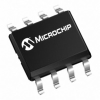
MCP1612-ADJI/MS Microchip Technology, MCP1612-ADJI/MS Datasheet - Page 9

MCP1612-ADJI/MS
Manufacturer Part Number
MCP1612-ADJI/MS
Description
IC BUCK REG ADJ 1A 1.4MHZ 8MSOP
Manufacturer
Microchip Technology
Type
Step-Down (Buck)r
Datasheet
1.MCP1612-ADJIMS.pdf
(22 pages)
Specifications of MCP1612-ADJI/MS
Package / Case
8-MSOP, Micro8™, 8-uMAX, 8-uSOP,
Internal Switch(s)
Yes
Synchronous Rectifier
Yes
Number Of Outputs
1
Voltage - Output
0.8 ~ 5 V
Current - Output
1A
Frequency - Switching
1.4MHz
Voltage - Input
2.7 ~ 5.5 V
Operating Temperature
-40°C ~ 85°C
Mounting Type
Surface Mount
Output Voltage
0.8 V to 5.5 V
Output Current
1 A
Input Voltage
2.7 V to 5.5 V
Switching Frequency
1.4 MHz
Operating Temperature Range
- 40 C to + 85 C
Mounting Style
SMD/SMT
Duty Cycle (max)
100 %
Lead Free Status / RoHS Status
Lead free / RoHS Compliant
Power - Output
-
Lead Free Status / Rohs Status
Lead free / RoHS Compliant
Available stocks
Company
Part Number
Manufacturer
Quantity
Price
Company:
Part Number:
MCP1612-ADJI/MS
Manufacturer:
MICROCHIP
Quantity:
12 000
Part Number:
MCP1612-ADJI/MS
Manufacturer:
MICROCHIP/微芯
Quantity:
20 000
3.0
The descriptions of the pins are listed in Table 3-1.
TABLE 3-1:
3.1
Connect the input voltage source to V
operation, the voltage on V
and +5.5V. A 10 µF bypass capacitor should be
connected between V
3.2
V
voltage is derived by filtering the V
3.3
Connect SHDN to a logic-level input in order to turn the
regulator on or off. A logic-high (>45% of V
enable the regulator. A logic-low (<15% of V
force the regulator into Shutdown mode. When in
shutdown, both the P-channel and N-channel switches
are turned off.
3.4
COMP is the internal transconductance amplifier
output pin. External compensation is connected to
COMP for control-loop stabilization.
© 2005 Microchip Technology Inc.
CC
Pin No.
provides bias for internal analog functions. This
1
2
3
4
5
6
7
8
MCP1612 PIN DESCRIPTIONS
Input Voltage Pin (V
Analog Input Voltage Pin (V
Shutdown Input Pin (SHDN)
Compensation Pin (COMP)
COMP
SHDN
Name
A
P
PIN FUNCTION TABLE
V
V
FB
GND
GND
L
CC
IN
X
IN
and P
IN
Input Voltage Pin
Analog Input Voltage Pin
Shutdown Control Input Pin
Transconductance Amplifier Output Pin
Feedback Input Pin
Analog Ground Pin
Power Ground Pin
Buck Inductor Output Pin
should be between +2.7V
GND
.
IN
IN
supply.
)
IN
. For normal
CC
IN
IN
)
) will
) will
3.5
Connect the output voltage of the buck converter
through an external resistor divider to FB to regulate
the output voltage. The nominal voltage compared to
this input for pulse termination is 0.8V.
3.6
Tie all small-signal ground returns to A
A
measurements.
3.7
Connect all large-signal ground returns to P
large-signal traces should have a small loop area and
length to prevent coupling of switching noise to
sensitive traces.
3.8
Connect L
carries large signal-level currents; all connections
should be made as short as possible.
GND
Function
can effect the sensitive internal analog
Feedback Pin (FB)
Analog Ground Pin (A
Power Ground Pin (P
Buck Inductor Output Pin (L
X
directly to the buck inductor. This pin
MCP1612
GND
DS21921B-page 9
GND
GND
)
)
GND
. Noise on
X
. These
)


