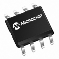
MCP1612-ADJI/MS Microchip Technology, MCP1612-ADJI/MS Datasheet - Page 5

MCP1612-ADJI/MS
Manufacturer Part Number
MCP1612-ADJI/MS
Description
IC BUCK REG ADJ 1A 1.4MHZ 8MSOP
Manufacturer
Microchip Technology
Type
Step-Down (Buck)r
Datasheet
1.MCP1612-ADJIMS.pdf
(22 pages)
Specifications of MCP1612-ADJI/MS
Package / Case
8-MSOP, Micro8™, 8-uMAX, 8-uSOP,
Internal Switch(s)
Yes
Synchronous Rectifier
Yes
Number Of Outputs
1
Voltage - Output
0.8 ~ 5 V
Current - Output
1A
Frequency - Switching
1.4MHz
Voltage - Input
2.7 ~ 5.5 V
Operating Temperature
-40°C ~ 85°C
Mounting Type
Surface Mount
Output Voltage
0.8 V to 5.5 V
Output Current
1 A
Input Voltage
2.7 V to 5.5 V
Switching Frequency
1.4 MHz
Operating Temperature Range
- 40 C to + 85 C
Mounting Style
SMD/SMT
Duty Cycle (max)
100 %
Lead Free Status / RoHS Status
Lead free / RoHS Compliant
Power - Output
-
Lead Free Status / Rohs Status
Lead free / RoHS Compliant
Available stocks
Company
Part Number
Manufacturer
Quantity
Price
Company:
Part Number:
MCP1612-ADJI/MS
Manufacturer:
MICROCHIP
Quantity:
12 000
Part Number:
MCP1612-ADJI/MS
Manufacturer:
MICROCHIP/微芯
Quantity:
20 000
DC CHARACTERISTICS (CONTINUED)
TEMPERATURE SPECIFICATIONS
© 2005 Microchip Technology Inc.
Electrical Specifications: Unless otherwise noted, V
I
Protection Features
Undervoltage Lockout
Undervoltage Lockout Hysteresis
Thermal Shutdown
Thermal Shutdown Hysteresis
Interface Signal (SHDN)
Logic-High Input
Logic-Low Input
Note 1:
Electrical Specifications: V
Temperature Ranges
Storage Temperature Range
Maximum Junction Temperature
Operating Junction Temperature Range
Thermal Package Resistances
Thermal Resistance, 8L-MSOP
Thermal Resistance, 8L-DFN
LOAD
= 100 mA, T
2:
Parameters
The integrated MOSFET switches have an integral diode from the L
these diodes are forward-biased, the package power dissipation limits must be adhered to. Thermal protection is not
able to regulate the junction temperature for these cases.
UVLO is specified for a falling V
return to operation.
Parameters
A
= +25°C. Boldface specifications apply over the T
IN
= 3.0V to 5.5V, F
UVLO-
T
V
V
SHD-HYS
UVLO
IN-HIGH
T
IN-LOW
Sym
SHD
HYS
IN
. Once the UVLO is activated, the UVLO-
Sym
T
T
T
JA
JA
OSC
A
A
J
Min
2.4
45
—
—
—
—
= 1 MHz with 10% Duty Cycle, C
IN
= V
Min
- 40
-65
—
—
—
CC
= V
2.55
Typ
200
160
—
—
9
SHDN
Typ
208
41
—
—
—
A
= 3.3V, V
range of -40°C to +85°C.
Max
2.7
—
—
—
—
15
+ 125
+150
+150
Max
—
—
X
OUT
pin to V
% of V
% of V
Units
Units
IN
°C/W
°C/W
= 1.8V, C
mV
°C
°C
HYS
V
°C
°C
°C
= 0.1 µF. T
IN
IN
IN
must be overcome before the device will
and from L
Note 2
Note 1
Continuous
Transient Only
Continuous Operation
Typical 4-layer board interconnecting
vias
Typical 4-layer board interconnecting
vias
IN
= C
A
= -40°C to +125°C.
OUT
X
MCP1612
to P
= 10 µF, L = 3.3 µH,
Conditions
Conditions
GND
. In cases where
DS21921B-page 5


