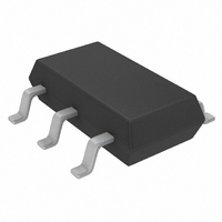
LTC3803ES6#TRMPBF Linear Technology, LTC3803ES6#TRMPBF Datasheet - Page 11

LTC3803ES6#TRMPBF
Manufacturer Part Number
LTC3803ES6#TRMPBF
Description
IC FLYBACK SYNC ADJ 1A TSOT23-6
Manufacturer
Linear Technology
Type
Flybackr
Datasheet
1.LTC3803HS6TRMPBF.pdf
(16 pages)
Specifications of LTC3803ES6#TRMPBF
Internal Switch(s)
No
Synchronous Rectifier
No
Number Of Outputs
1
Voltage - Output
Adjustable
Current - Output
1A
Frequency - Switching
200kHz
Voltage - Input
Adjustable
Operating Temperature
-40°C ~ 85°C
Mounting Type
Surface Mount
Package / Case
TSOT-23-6, TSOT-6
Dc To Dc Converter Type
FLYBACK CONTROLLER
Pin Count
6
Output Current
1A
Package Type
TSOT-23
Mounting
Surface Mount
Operating Temperature Classification
Automotive
Operating Temperature (min)
-40C
Operating Temperature (max)
125C
Lead Free Status / RoHS Status
Lead free / RoHS Compliant
Power - Output
-
Lead Free Status / Rohs Status
Compliant
Other names
LTC3803ES6#PBF
LTC3803ES6#PBF
LTC3803ES6#PBF
Available stocks
Company
Part Number
Manufacturer
Quantity
Price
APPLICATIONS INFORMATION
and the V
the V
situation, this may result in either several on-off cycles
before proper operation is reached or permanent relaxation
oscillation at the V
Component selection is as follows:
Resistor R
worst-case minimum charging current greater than the
maximum rated LTC3803 start-up current, to ensure there
is enough current to charge C
old. It should be made large enough to yield a worst-case
maximum charging current less than the minimum rated
LTC3803 supply current, so that in operation, most of the
LTC3803’s supply current is delivered through the third
winding. This results in the highest possible effi ciency.
Capacitor C
the relaxation oscillation behavior described above. This
is complicated to determine theoretically as it depends on
the particulars of the secondary circuit and load behavior.
Empirical testing is recommended.
The third transformer winding should be designed so that
its output voltage, after accounting for the D2’s forward
voltage drop, exceeds the maximum V
Also, the third winding’s nominal output voltage should
be at least 0.5V below the minimum rated V
age to avoid running up against the LTC3803’s V
regulator, needlessly wasting power.
V
In applications including a third transformer winding,
the internal V
LTC3803 from overvoltage transients as the third wind-
ing is powering up.
In applications where a third transformer winding is
undesirable or unavailable, the shunt regulator allows
the LTC3803 to be powered through a single dropping
resistor from V
capacitor, C
Figure 3). This simplicity comes at the expense of reduced
effi ciency due to the static power dissipation in the R
dropping resistor.
CC
SHUNT REGULATOR
CC
turn-on threshold. Depending on the particular
CC
START
VCC
VCC
node begins to charge via R
CC
should then be made large enough to avoid
, that closely decouples V
IN
should be made small enough to yield a
shunt regulator serves to protect the
CC
to V
node.
CC
, in conjunction with a bypass
VCC
to the V
CC
turn-off threshold.
CC
START
CC
turn-on thresh-
CC
to GND (see
clamp volt-
back up to
CC
shunt
VCC
The shunt regulator can draw up to 25mA through the
V
regulate V
is low enough such that the static power dissipation in
R
simplest way to power the LTC3803.
EXTERNAL PREREGULATOR
The circuit in Figure 4 shows a third way to power the
LTC3803. An external series preregulator consisting of
series pass transistor Q1, Zener diode D1, and bias resis-
tor R
maximum rated V
momentarily charges the V
threshold, enabling the LTC3803.
Figure 3. Powering the LTC3803 Via the Internal Shunt Regulator
CC
VCC
Figure 4. Powering the LTC3803 with an External Preregulator
pin to GND to drop enough voltage across R
B
is acceptable, using the V
brings V
CC
to around 9.5V. For applications where V
R
CC
B
D1
8.2V
to at least 7.6V nominal, well above the
CC
V
V
IN
IN
turn-off threshold. Resistor R
R
Q1
VCC
C
VCC
CC
R
V
START
C
CC
node up to the V
VCC
LTC3803
GND
CC
3803 F03
shunt regulator is the
V
CC
LTC3803
GND
LTC3803
3803 F04
CC
turn-on
11
VCC
START
3803fc
to
IN


